

Contact barrier layer deposition process
a technology of contact barrier layer and deposition process, which is applied in the direction of basic electric elements, semiconductor/solid-state device manufacturing, electrical equipment, etc., can solve the problems of affecting the reliability of the resulting ics, uniform tin layer being deposited across the si substrate surface,
- Summary
- Abstract
- Description
- Claims
- Application Information
AI Technical Summary
Problems solved by technology
Method used
Image

Examples
Embodiment Construction
.”
BRIEF DESCRIPTION OF THE DRAWINGS
[0014]For a more complete understanding of the principles disclosure herein, and the advantages thereof, reference is now made to the following descriptions taken in conjunction with the accompanying drawings, in which:
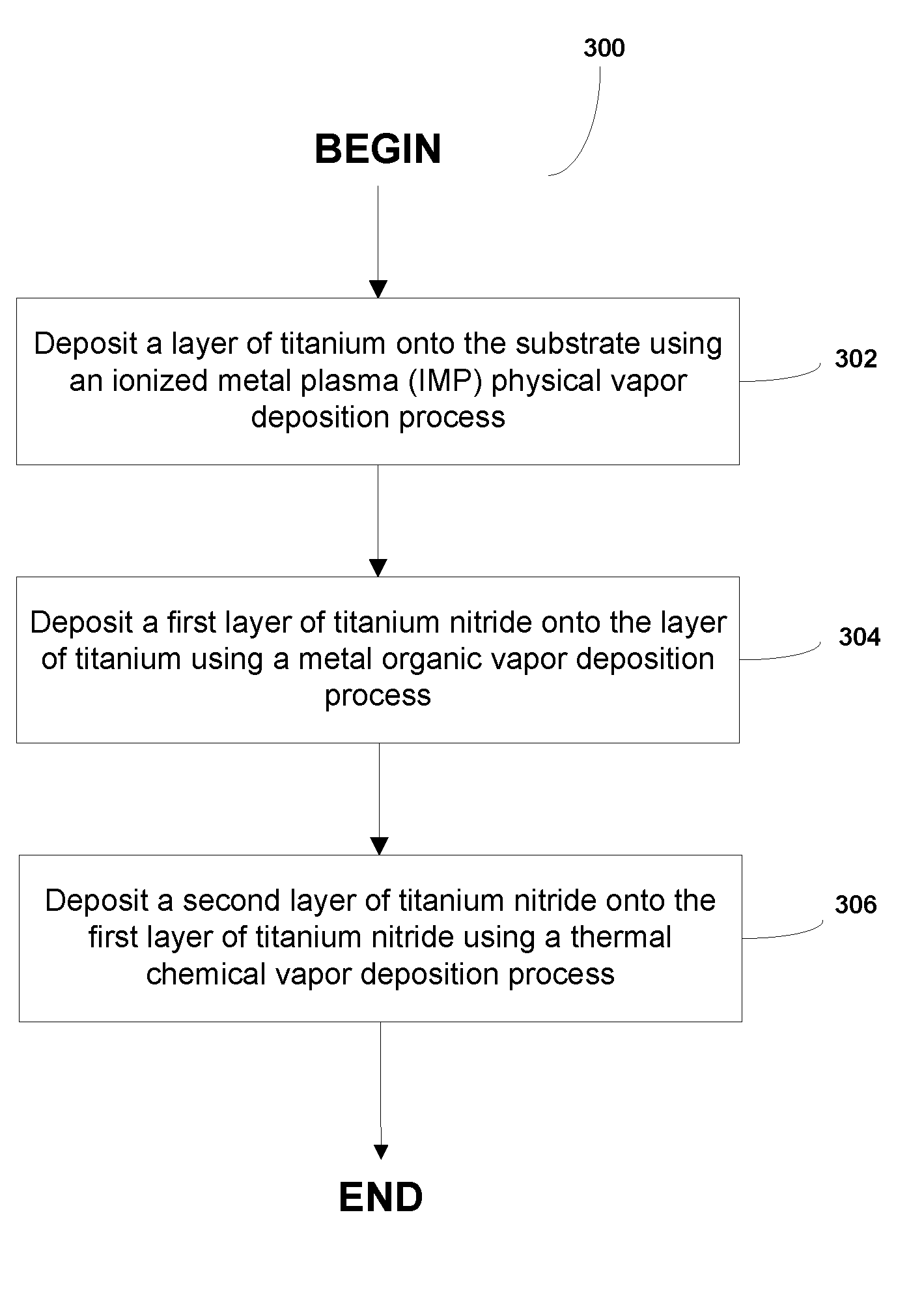
[0015]FIG. 1 is a cross-sectional illustration of the various sub-layers of material that form a barrier layer over a semiconductor substrate, in accordance with one embodiment.
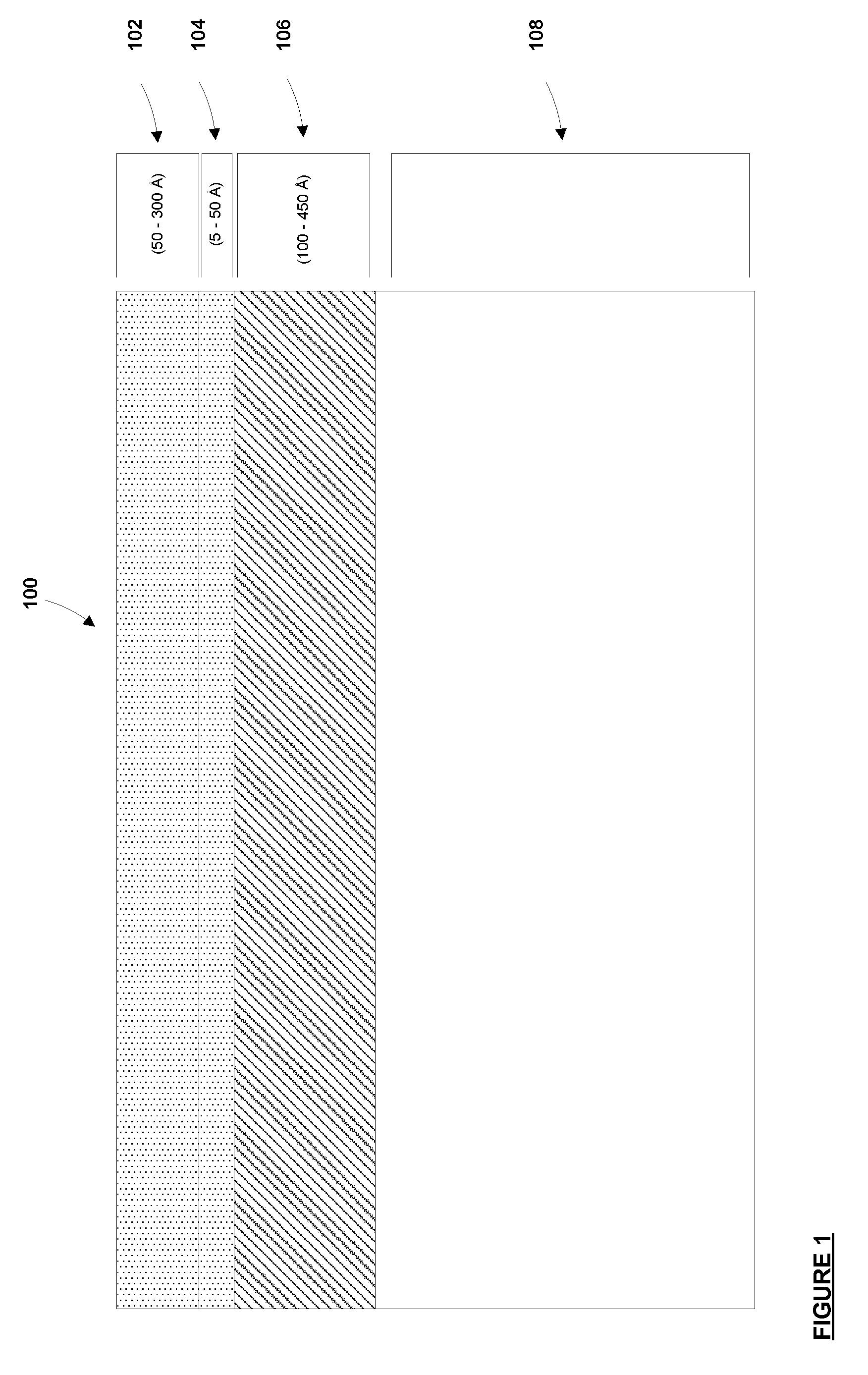
[0016]FIG. 2 is a top level illustration of a system for depositing a “mixed type” contact barrier layer onto a semiconductor substrate, in accordance with one embodiment.
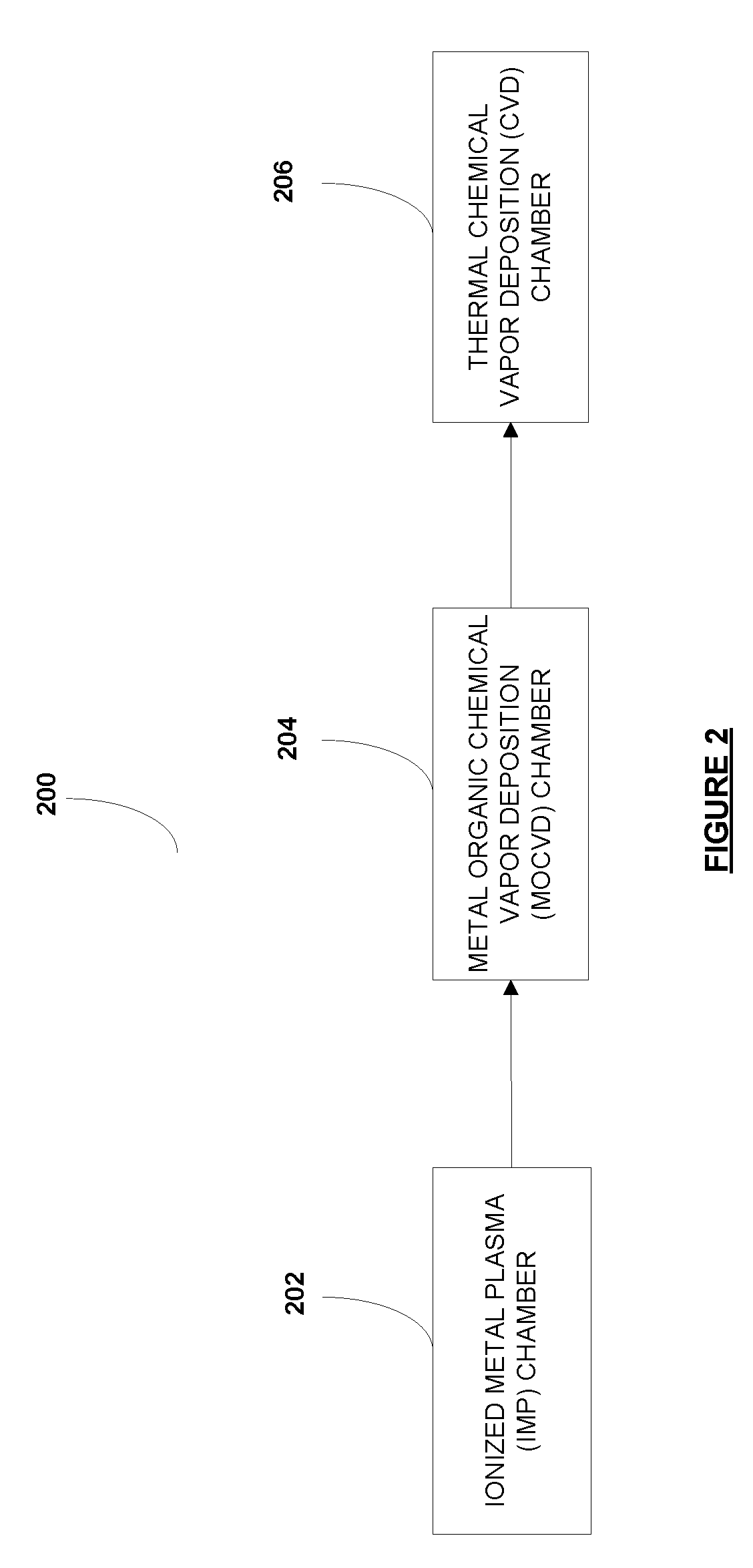
[0017]FIG. 3A is a flowchart of a method to form a new contact barrier layer onto a semiconductor substrate, in accordance with one embodiment.
[0018]FIG. 3B is a flowchart detailing the operation of the ionized metal plasma (IMP) physical vapor deposition chamber to form a layer of Ti on a semiconductor substrate, in accordance with one embodiment.
[0019]FIG. 3C is a flowchart detailing the op...
PUM
 Abstract
Description
Claims
Application Information