Semiconductor substrate having a protection layer at the substrate back side

a technology of silicon-based substrates and protection layers, applied in the field of silicon-based substrates, can solve the problems of difficult control of factors, high uncontrollable affecting subsequent processes, and defocused exposure fields, so as to reduce influence, reduce non-uniformities, and improve surface characteristics

Inactive Publication Date: 2008-06-05
TAIWAN SEMICON MFG CO LTD
View PDF2 Cites 12 Cited by
  • Summary
  • Abstract
  • Description
  • Claims
  • Application Information

AI Technical Summary

Benefits of technology

[0010]Generally, the subject matter disclosed herein is related to a technique for reducing influences caused by non-uniformities generated at the back side of a substrate during the processing of microstructure devices. To this end, the respective back side of the substrate under consideration may be efficiently protected, at least prior to manufacturing processes which typically may affect the back side. The protection of the back side may be accomplished on the basis of an appropriate protective material that may enable the reduction of non-uniformities at the back side, which may be caused by deposition-related contaminations and the like, wherein, after the corresponding treatment, superior surface characteristics may be established compared to a non-protected back side as is used in conventional techniques. Consequently, the further manufacturing sequence may be continued on the basis of significantly reduced non-uniformities or on the basis of well-defined surface characteristics with respect to defectivity, surface roughness, chemical composition and the like, thereby significantly enhancing the overall process result in the subsequent manufacturing stages. In some illustrative embodiments, the corresponding protective material may comprise a highly inert material composition, which may have a high resistivity against a plurality of reactive etch ambients, such as wet chemical etch ambients typically used in a plurality of manufacturing stages for removing unwanted material portions from the back side. Any etch damage, which may typically be caused in conventional strategies and which may therefore result in corresponding non-uniformities, may be significantly reduced by the protective material, thereby enhancing the performance of further critical processes such as lithography processes, metallization processes and the like.
[0011]According to one illustrative embodiment disclosed herein, a method comprises forming a protection layer on a back side of a substrate, wherein the substrate has a front side for forming therein and thereon microstructure features. The method further comprises performing at least one manufacturing process for forming a microstructure feature on the front side of the substrate. Finally, the method comprises removing material from above the back side during the at least one manufacturing process using the protection layer as a barrier against damaging of the back side.

Problems solved by technology

Thus, economic constraints drive semiconductor manufacturers to steadily increase the substrate dimensions, thereby also increasing the area available for producing actual semiconductor devices.
For example, the presence of particles on the back side may result in defocused exposure fields due to the reduced depth of focus.
In conventional process strategies, these factors may be difficult to be controlled, since many of the processes, such as deposition processes, wet chemical processes and the like, may also affect the back side of the substrate, however, in a highly unpredictable manner.
Other deposition processes may be chemical vapor deposition (CVD), physical vapor deposition (PVD) and the like, which may result in a highly unpredictable coverage of portions of the back side, thereby affecting subsequent processes in a highly uncontrollable manner.
Consequently, with increasing dimensions of the substrates used in fabricating microstructures and the continuous demand for reduced critical dimensions of the individual features, the characteristics of the substrate back side may have an increasing influence on production yield, wherein presently practiced process strategies may suffer from insufficient controllability of the properties of the substrate back side.

Method used


Image

  • Semiconductor substrate having a protection layer at the substrate back side
  • Semiconductor substrate having a protection layer at the substrate back side
  • Semiconductor substrate having a protection layer at the substrate back side

Examples


Embodiment Construction

[0020]Various illustrative embodiments of the invention are described below. In the interest of clarity, not all features of an actual implementation are described in this specification. It will of course be appreciated that in the development of any such actual embodiment, numerous implementation-specific decisions must be made to achieve the developers' specific goals, such as compliance with system-related and business-related constraints, which will vary from one implementation to another. Moreover, it will be appreciated that such a development effort might be complex and time-consuming, but would nevertheless be a routine undertaking for those of ordinary skill in the art having the benefit of this disclosure.

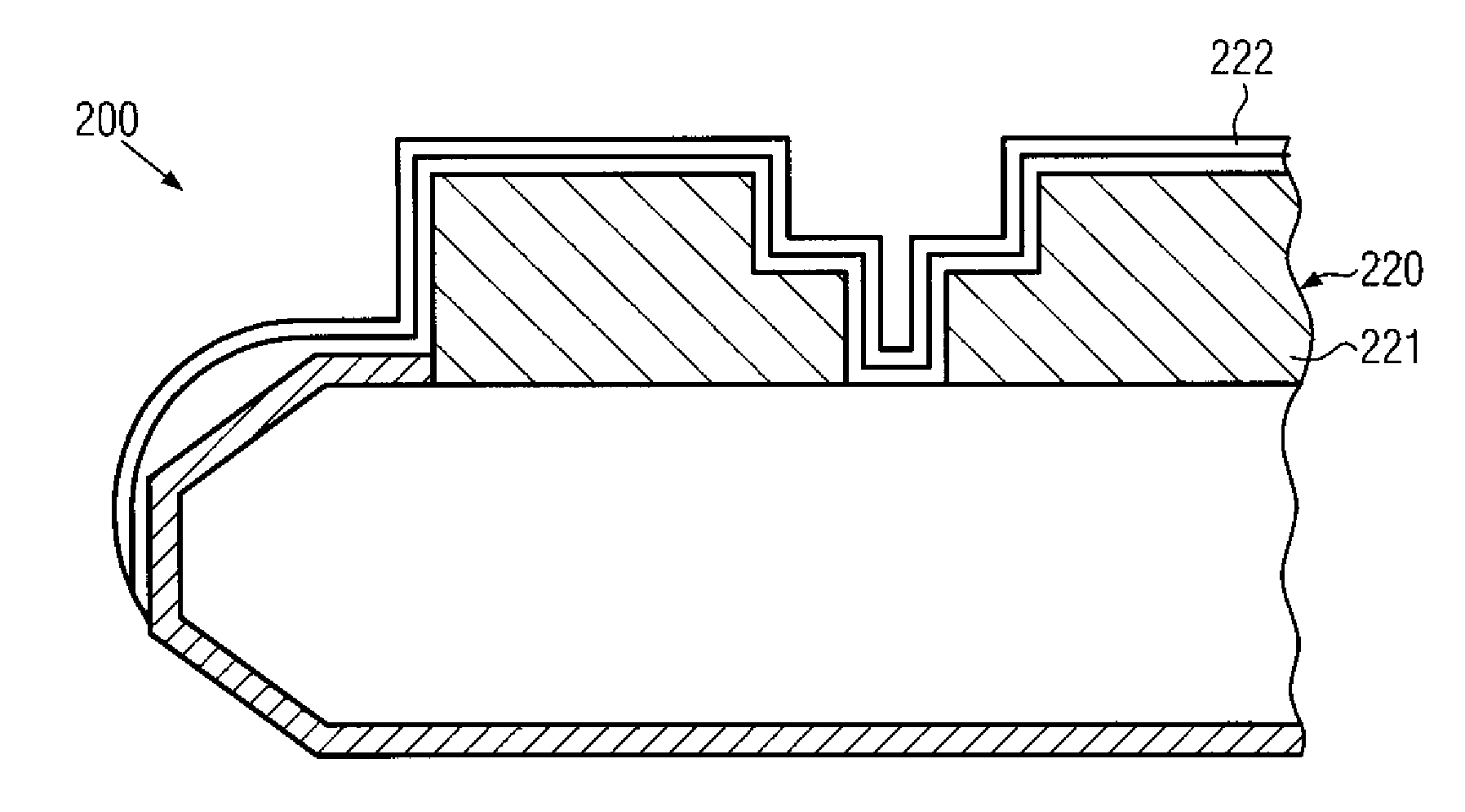
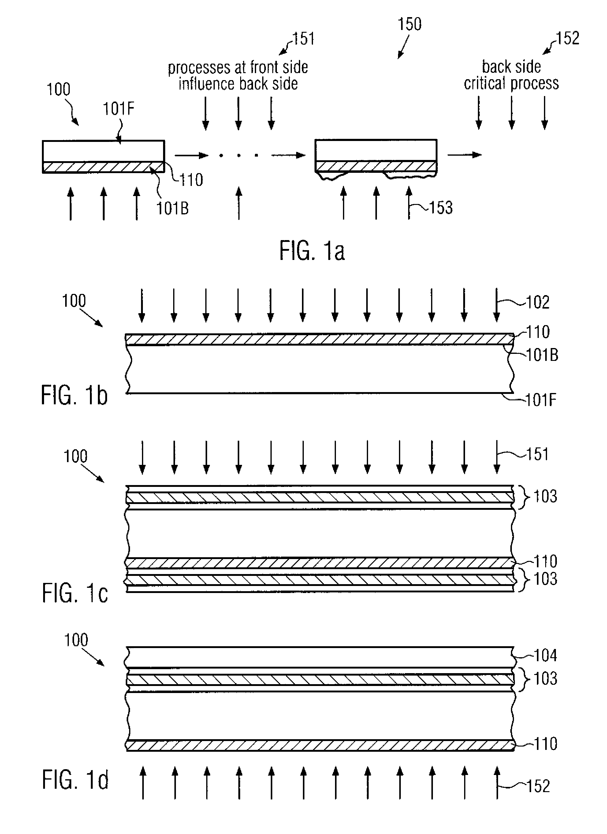
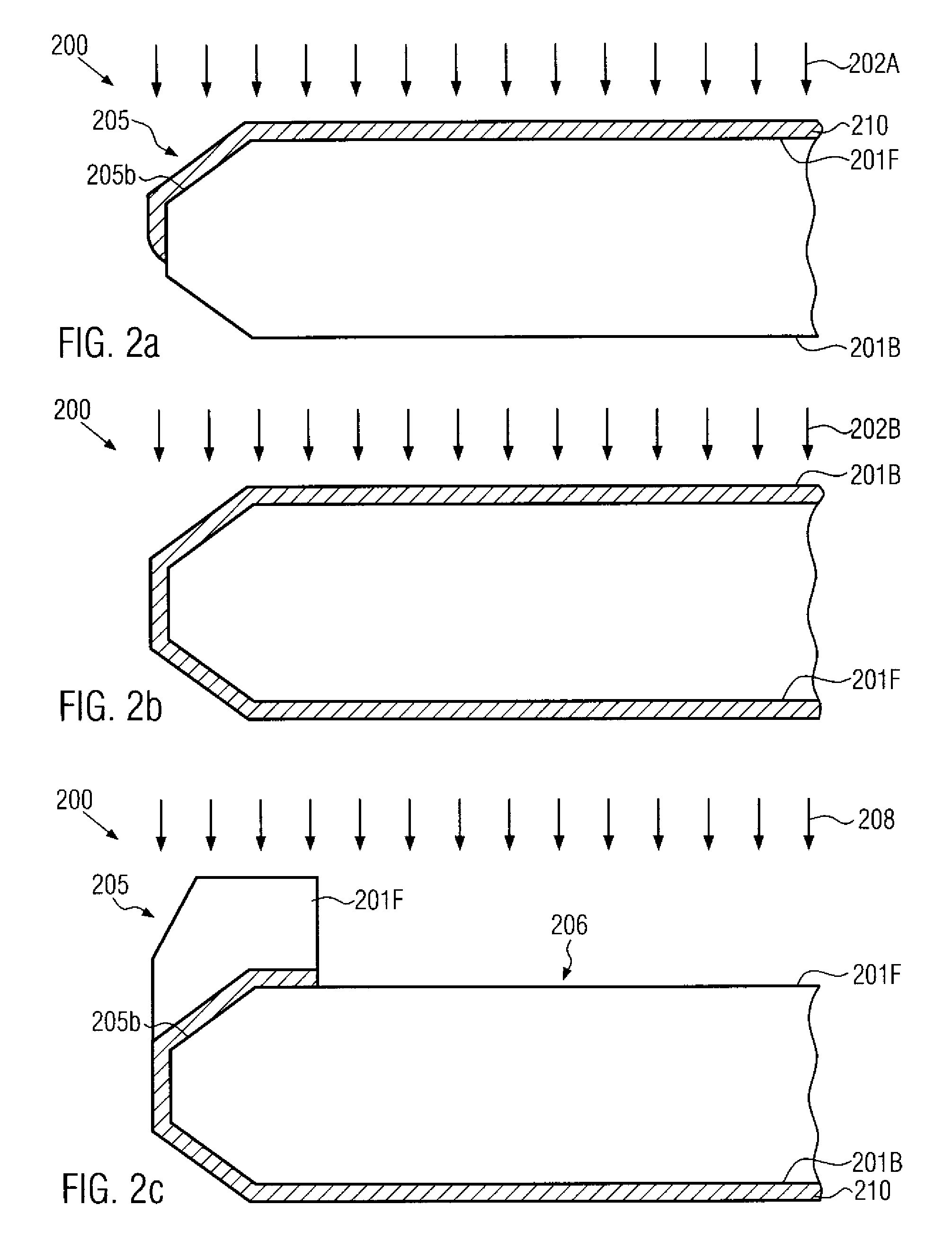
[0021]The present subject matter will now be described with reference to the attached figures. Various structures, systems and devices are schematically depicted in the drawings for purposes of explanation only and so as to not obscure the present disclosure with details ...


PUM

PropertyMeasurementUnit
microstructureaaaaaaaaaa
etch rateaaaaaaaaaa
resistivityaaaaaaaaaa

Abstract

By forming a protection layer on the back side of a substrate prior to any process sequences, which may deposit material or material residues on the back side, the respective back side uniformity may be significantly enhanced, thereby also increasing process efficiency of subsequent back side critical processes, such as lithography, back end of line processes and the like. In one illustrative embodiment, silicon carbide may be used as a material for forming a respective protection layer.

Description

BACKGROUND OF THE INVENTION[0001]1. Field of the Invention[0002]Generally, the present disclosure relates to the fabrication of integrated circuits, and, more particularly, to techniques for enhancing the overall process flow by considering characteristics of the back side of substrates during various manufacturing stages.[0003]2. Description of the Related Art[0004]Semiconductor devices are typically formed on substantially disc-shaped substrates made of any appropriate material. One prominent type of semiconductor material is silicon, since the majority of semiconductor devices including highly complex electronic circuits is currently, and in the foreseeable future will be, manufactured on the basis of silicon, thereby rendering silicon substrates and silicon-containing substrates, such as silicon-on-insulator (SOI) substrates, viable carriers for forming semiconductor devices, such as microprocessors, SRAMs, ASICs (application specific ICs) and the like. The individual integrated...

Claims


Application Information

Patent Timeline
Patent Type & Authority Applications(United States)
IPC IPC(8): H01L21/311B32B9/04
CPCH01L2924/1433H01L23/296H01L2924/0002H01L2924/00
Inventor LETZ, TOBIASSCHUEHRER, HOLGERNOPPER, MARKUS
Owner TAIWAN SEMICON MFG CO LTD
Why Eureka
Try Eureka