
Semiconductor package and method of manufacturing the same

Inactive Publication Date: 2008-06-12
SAMSUNG ELECTRONICS CO LTD
View PDF15 Cites 6 Cited by
  • Summary
  • Abstract
  • Description
  • Claims
  • Application Information

AI Technical Summary

Benefits of technology

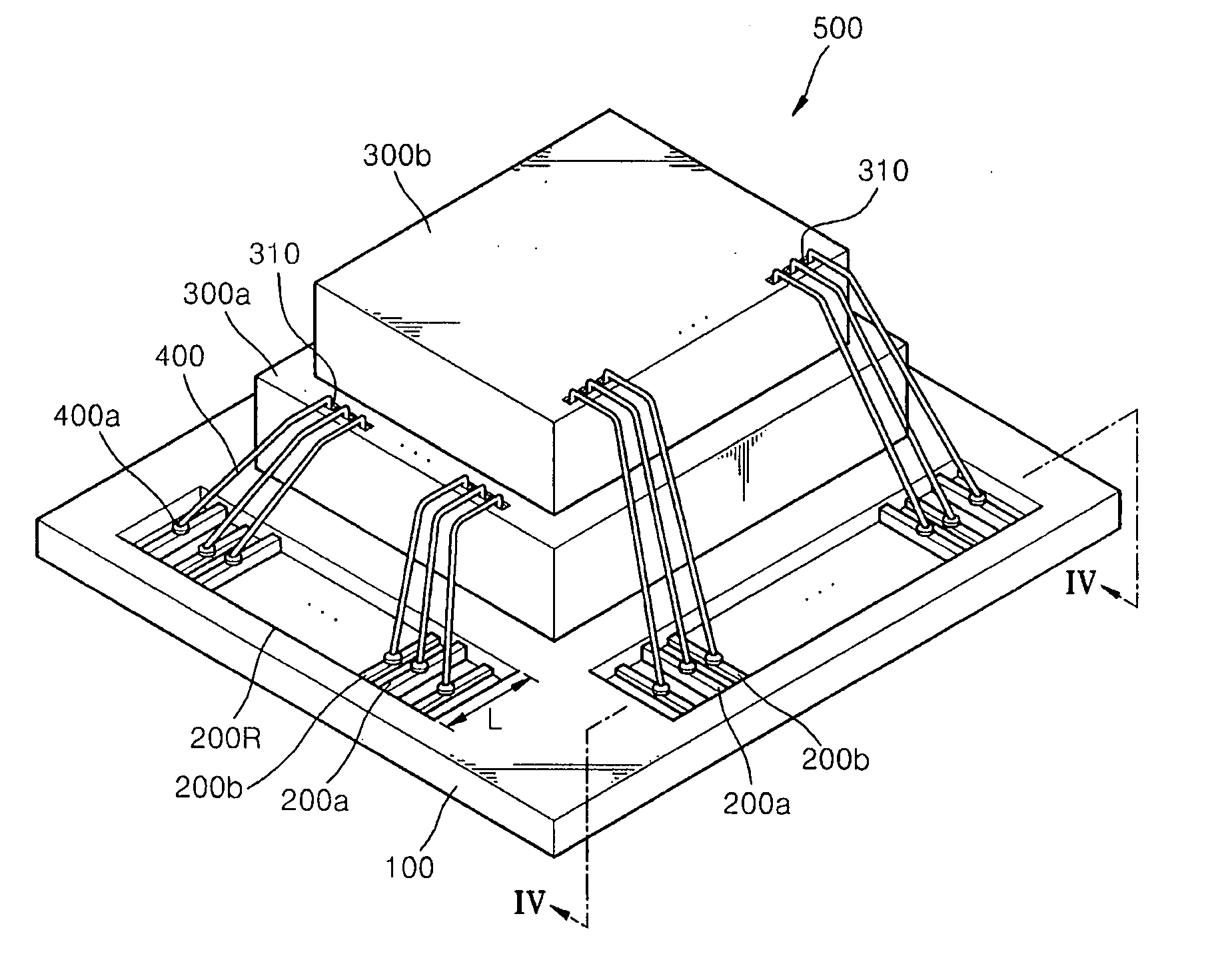
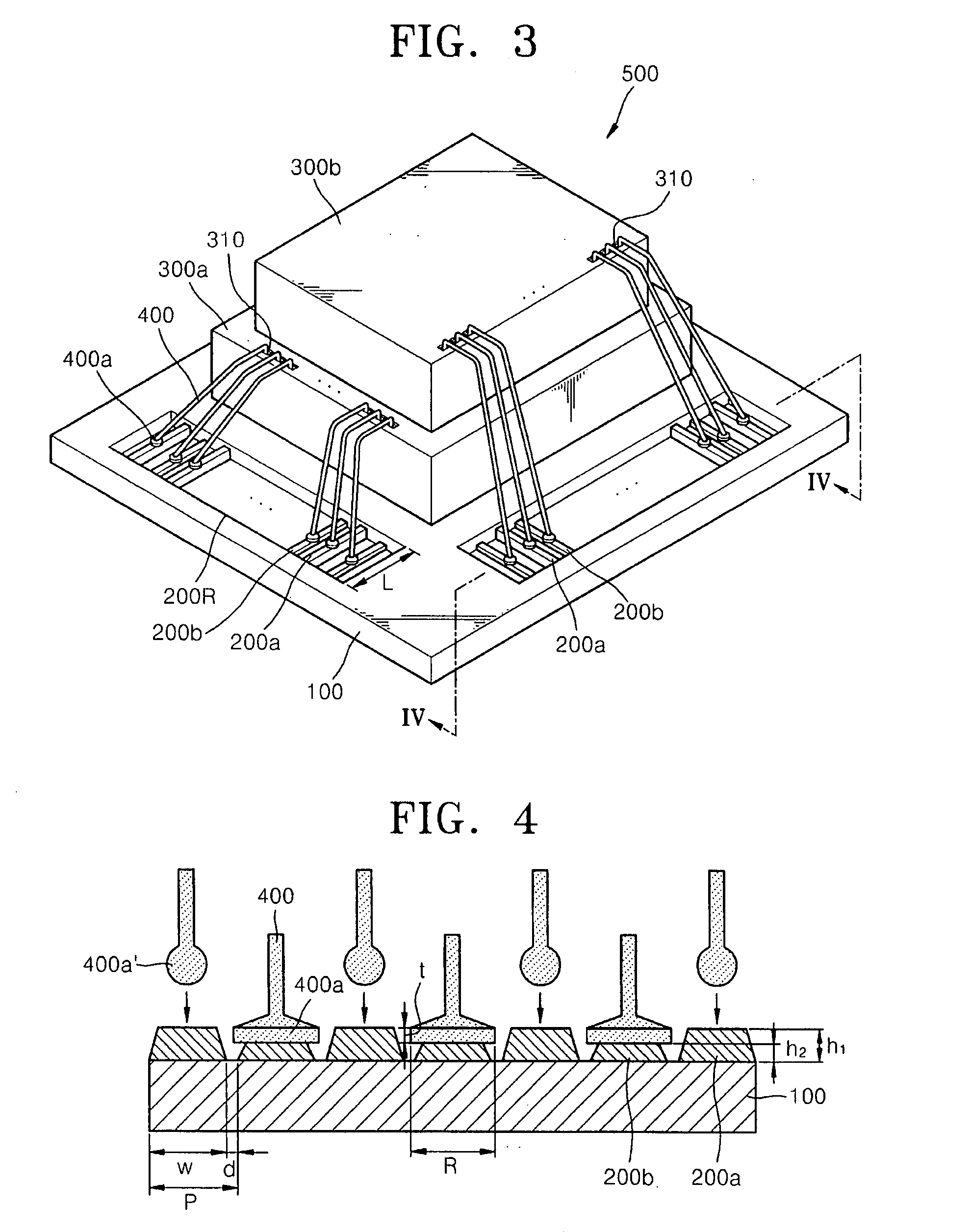
[0012]In accordance with the present invention, a semiconductor package can be provided that realizes sufficient bond strength between a conductive pattern and a wire, in spite of a reduction in the pitch of the wirings in the semiconductor package due to miniaturization of the semiconductor package.
[0013]In accordance with the present invention, a method of manufacturing of a semiconductor package can be provided that does not cause short circuits between neighboring wirings and which can perform a wire boding process in spite of a reduction in the pitch of the wirings in the semiconductor package due to miniaturization of the semiconductor package.
[0014]In accordance with the present invention, although the pitch of the wirings is reduced due to miniaturization of the semiconductor package, a wire ball having a diameter that is of a critical value or greater can be applied in a bonding process, thereby ensuring a sufficient bond strength between the conductive patterns and the wires and reducing defects caused by short circuits between neighboring conductive patterns.

Problems solved by technology

However, the interconnection process with the solder bumps in CSP package cannot provide such a reliable and economical interconnection as a conventional wire bonding process.
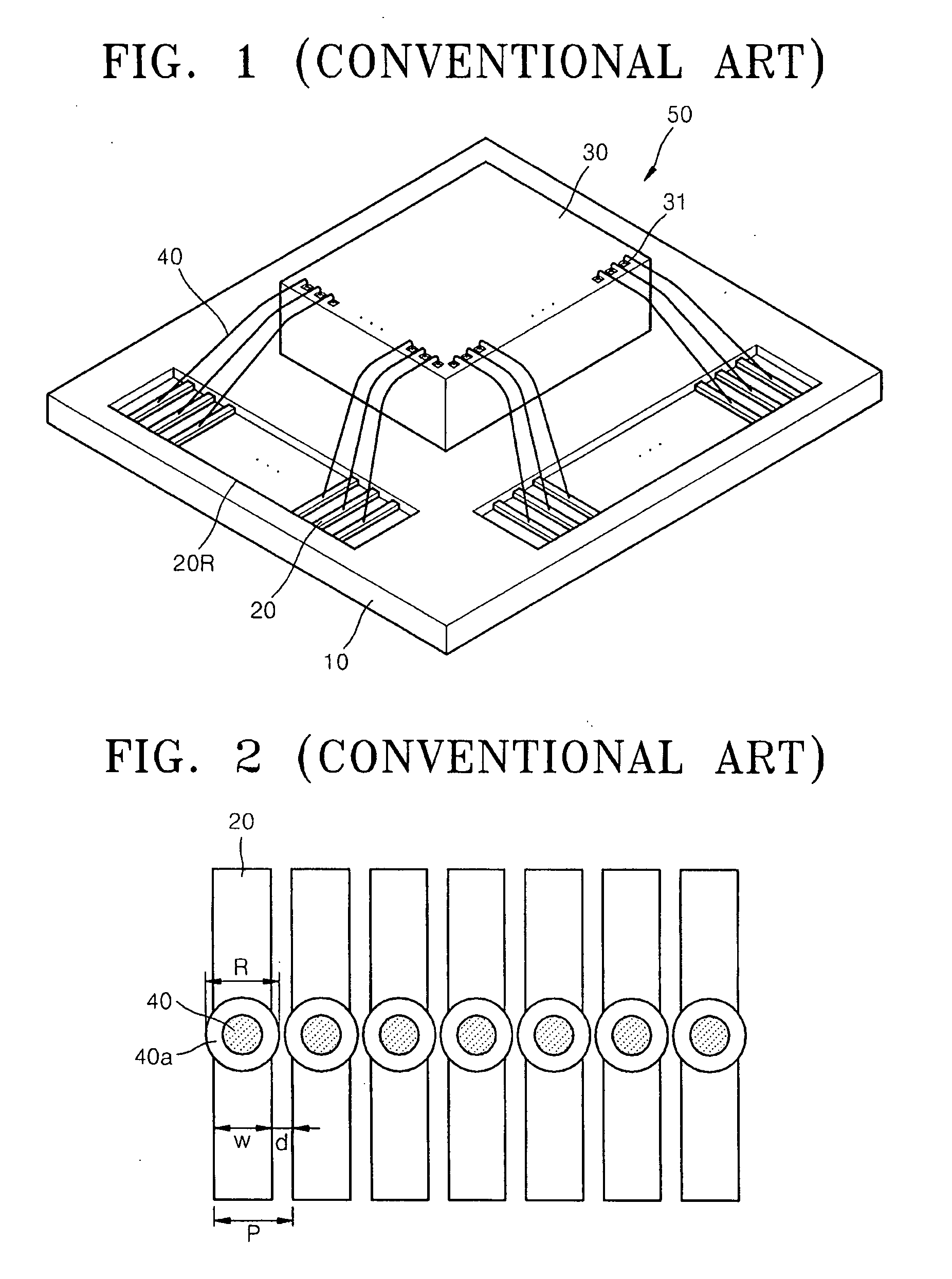
However, as the diameter of the wire decreases, a sweeping phenomenon of the wire 40 is caused during the subsequent transfer molding process of an epoxy resin, which can cause short circuit between the wires 40.
Thus, there is a limitation in reducing the critical value of the diameter R of the wire ball by reducing the diameter of the wires 40.
Accordingly, the number of defects of final products is increasing, and high precision wiring equipment for resolving this problem is becoming a serious factor in increasing manufacturing costs.

Method used


Image

  • Semiconductor package and method of manufacturing the same
  • Semiconductor package and method of manufacturing the same
  • Semiconductor package and method of manufacturing the same

Examples


Embodiment Construction

[0041]Hereinafter, aspect of the present invention will now be described more fully with reference to the accompanying drawings, in which exemplary embodiments of the invention are shown.

[0042]The invention can, however, be embodied in many different forms and should not be construed as being limited to the embodiments set forth herein. It will also be understood that when a layer is referred to as being “on” another layer or substrate, it can be directly on the other layer or substrate, or intervening layers or substrate can also be present. In the drawings, the thicknesses of layers and regions are exaggerated for clarity. Like reference numerals in the drawings denote like elements, and thus their description will be omitted. The term ‘and / or’ refers to one of or a combination of at least two of the listed items.

[0043]In the present description, terms such as ‘first’, ‘second’, etc. are used to describe various members, components, regions, layers, and / or portions. However, the m...


PUM


Abstract

Provided are a semiconductor package in which bonding pads of a semiconductor chip are electrically connected to interconnection portions by wire-bonding, and a method of manufacturing the semiconductor package. The semiconductor package includes: a substrate; an interconnection portion that is disposed on the substrate and comprises conductive patterns having a first thickness and conductive patterns having a second thickness that is smaller than the first thickness; at least one semiconductor chip that is mounted on the substrate and comprises a plurality of bonding pads; and a plurality of wires electrically connecting the conductive patterns and the bonding pads.

Description

CROSS-REFERENCE TO RELATED PATENT APPLICATION[0001]This application claims priority under 35 U.S.C. §119 to of Korean Patent Application No. 10-2006-0124063, filed on Dec. 7, 2006 in the Korean Intellectual Property Office, the disclosure of which is incorporated herein in its entirety by reference.BACKGROUND OF THE INVENTION[0002]1. Field of the Invention[0003]The present invention relates to a semiconductor package and a method of manufacturing the semiconductor package, and more particularly, to a semiconductor package in which a bonding pad of a semiconductor chip is electrically connected to an interconnection portion of the semiconductor package by wire bonding, and a method of manufacturing the semiconductor package.[0004]2. Description of the Related Art[0005]Electronic appliances are becoming smaller, higher capacity, and increasingly multi-functional, largely owing to the continued development in the field of semiconductor integration technology and electronic engineering....

Claims


Application Information

Patent Timeline
IPC IPC(8): H01L23/538H01L21/60
CPCH01L23/498H01L23/49838H01L2924/014H01L2924/01033H01L2924/01006H01L24/48H01L2924/01079H01L2924/01074H01L2924/01029H01L2924/01028H01L2924/01015H01L2225/0651H01L2224/85205H01L2224/49433H01L24/49H01L25/0657H01L25/50H01L2224/32145H01L2224/48091H01L2224/48095H01L2224/48465H01L2924/00014H01L2924/00H01L2924/15787H01L2224/05554H01L2924/181H01L2224/45099
Inventor OH, YUN-JIN
Owner SAMSUNG ELECTRONICS CO LTD
Learn More