Microminiature power converter and thin film magnetic induction device thereof

a technology of micro-miniature power converter and induction device, which is applied in the direction of transformer/inductance details, transformer/inductance coil/winding/connection, etc., can solve the problems of increasing manufacturing cost, reducing the packaging area of power modules, and affecting the efficiency of the power module, so as to reduce the induced voltage

Active Publication Date: 2008-06-12
FUJI ELECTRIC CO LTD
View PDF3 Cites 17 Cited by
  • Summary
  • Abstract
  • Description
  • Claims
  • Application Information

AI Technical Summary

Benefits of technology

[0014]One aspect of the present invention is the microminiature power converter. The power converter includes a semiconductor device having an integrated circuit, and a thin film magnetic induction device operatively connected to the semiconductor device. The thin film magnetic induction device includes a magnetic insulating substrate having a first principal plane and a second principal plane, a plurality of first through-holes, and a plurality of second through-holes. The induction device further includes a solenoid coil comprising a conductor extending on the first principal plane of the magnetic insulating substrate, passing through the through holes and extending on the second principal plane of the magnetic insulating substrate to form a coil configuration. Second connection conductors are in the second through-holes. A plurality of pairs of electrodes are connected through the second connection conductors and formed opposing each other on the first principal plane and the second principal plane. The second through-holes are situated along a peripheral region of the magnetic insulating substrate.
[0016]In another aspect, the magnetic insulating substrate has at least one of gaps or grooves around the peripheral region thereof to reduce induced voltage between the pairs of electrodes. The gaps can extend from the second through-holes or can be spaced from the second through-holes. Each of the gaps can have a slit configuration passing through the magnetic insulating substrate. The grooves can extend between adjacent pairs of the electrodes on the first or second principal plane. The grooves can extend from at least one the first or the second principal plane toward but not to the other of the first or second plane. The gaps or grooves can reach an outer peripheral end of the magnetic insulating substrate.

Problems solved by technology

Since discrete parts are packaged arranging on the same substrate, however, the reduction in packaging area of the power module is restricted.
Particularly, a magnetic part, such as an inductor or a transformer, takes up a significant amount of volume in comparison with an integrated circuit.
Forming such structure, however, requires a vacuum process, thus raising the manufacturing cost.
In addition, it needs to laminate a multiple of magnetic films and insulator films for use at high electric current, which increases the costs very much.
The decreased cross-sectional area of the coil conductor and the elongated conductor wire bring about an increase in the DC resistance of the coil conductor and an increase in power loss.
The size of the semiconductor element (IC chip 80), on the other hand, can be restricted by the performance.
Nevertheless, since the semiconductor element is mounted on the magnetic induction device and electrodes are arranged in the peripheral region, the size of the semiconductor element is eventually restricted by a size of the magnetic induction device.
When the thin film magnetic induction device is minimized in correspondence with the reduced size of the semiconductor element, the performance of the magnetic induction device becomes worse, resulting in degraded efficiency of the power converter.
Moreover, a large induced voltage is generated on the electrodes (a voltage generated by an action of magnetic field of the coil on the connection conductor of the electrodes), which is apt to bring about malfunctions of the semiconductor element (an IC).

Method used


Image

  • Microminiature power converter and thin film magnetic induction device thereof
  • Microminiature power converter and thin film magnetic induction device thereof
  • Microminiature power converter and thin film magnetic induction device thereof

Examples


first embodiment

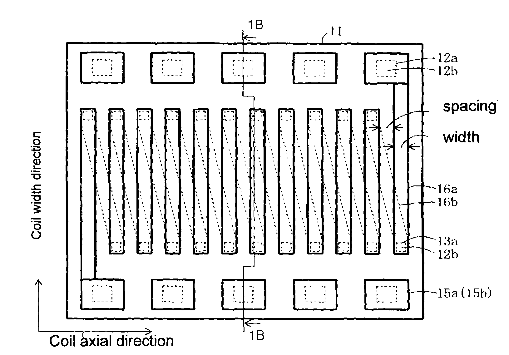
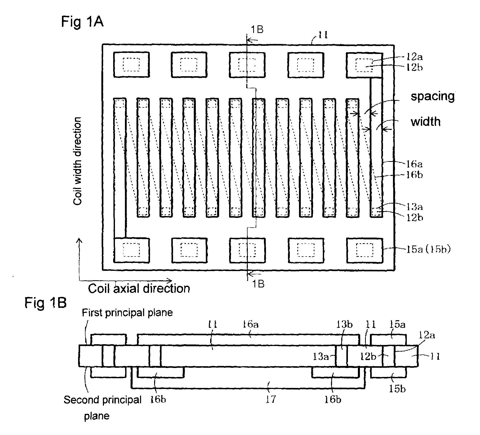
[0031]Referring to FIGS. 1A and 1B, although the microminiature power converter includes an IC chip and other components, as shown in FIG. 11, they are omitted in FIGS. 1A and 1B to show the thin film magnetic induction device. The thin film magnetic induction device comprises a ferrite substrate 11, which is a magnetic insulating substrate, a solenoid coil formed in the inner region of the ferrite substrate 11, pairs of electrodes arranged in the peripheral side region of the ferrite substrate 11 along the direction parallel to the axis of the coil, pairs of electrodes 15a and 15b opposing one another while sandwiching the ferrite substrate 11, and a protective film 17. The solenoid coil includes coil conductors 16a and 16b, and connection conductors 13b that electrically connect the coil conductors 16a and 16b to form a coil configuration. Connection conductors 12b electrically connect the electrodes 15a and 15b. The connection conductors 12b and 13b are provided by forming conduc...

third embodiment

[0053]In the alternative embodiment of FIGS. 6A and 6B, the electrodes 15a, 15b are drawn inwardly from the outer peripheral end. However, as provided in the third embodiment, the electrodes 15a, 15b can extend to the outer peripheral end without negating the advantages.

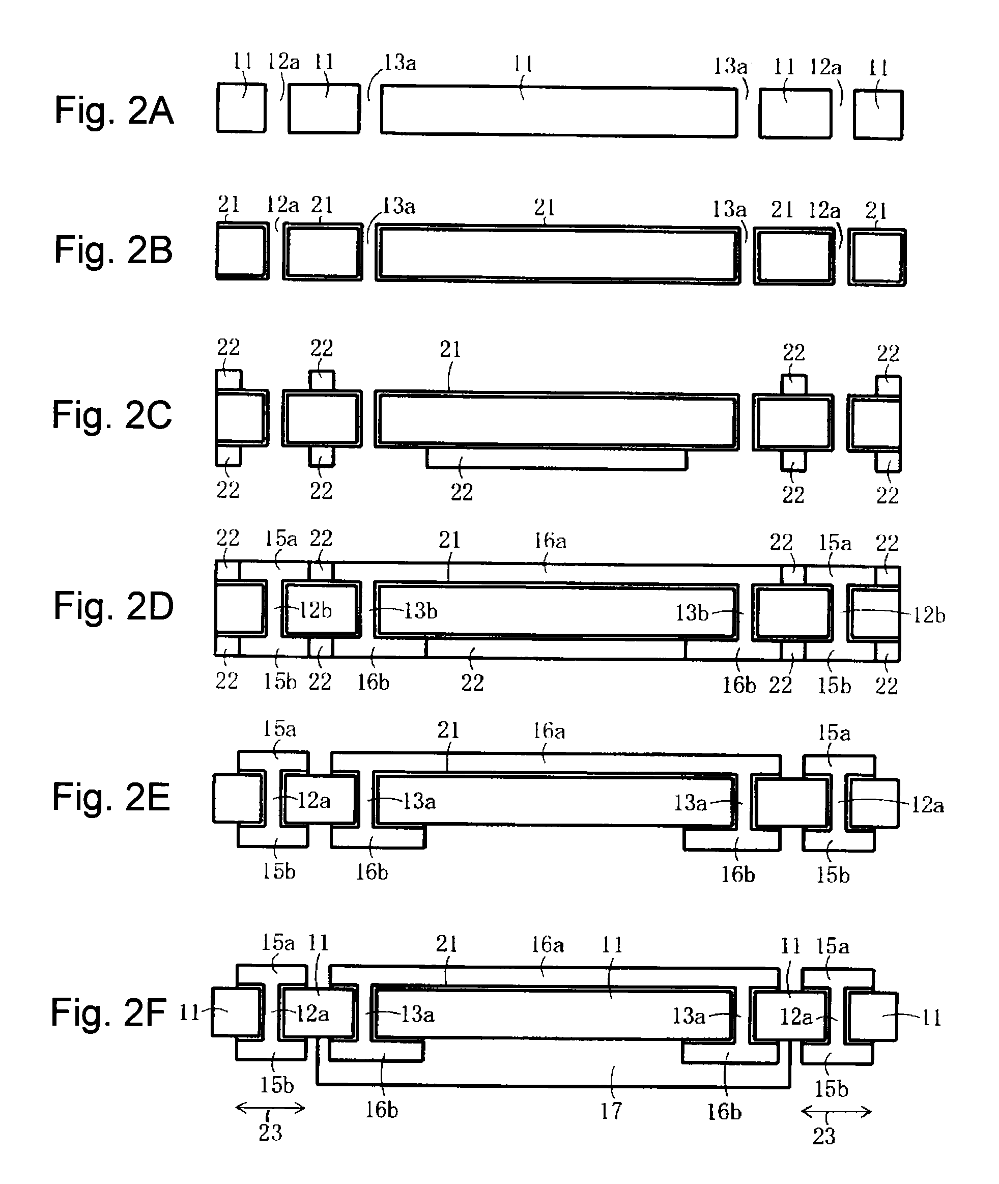
[0054]FIGS. 8A, 8B, 8C show the fourth embodiment of a microminiature power converter. In the fourth embodiment, a groove 70 with a slit shape that does not pass throughout the ferrite substrate 11 extends from the through-hole 12a connecting the electrode 15a on the first principal plane and the electrode 15b on the second principal plane to the outer peripheral end of the substrate. Thus, part of the ferrite substrate 11 outside the electrodes 15a, 15b is decreased, thereby reducing the outer peripheral magnetic flux 43 flowing outside the electrodes 15a, 15b. To fabricate the fourth embodiment, again, only the patterning step (FIG. 2A) of forming the through-holes in the ferrite substrate in the steps (FIGS. 2A-2F...


PUM


Abstract

A microminiature power converter includes a thin film magnetic induction device including a ferrite substrate and a solenoid coil conductor extending along the first and second principal planes of the substrate with the conductor extending through through-holes formed in the substrate to form a coil configuration. Electrodes are positioned near the peripheral region of the substrate and are collectively arranged at least one along the direction parallel to the axis of the solenoid coil formed by the conductor. The length of the coil can be increased to increase the inductance value of the coil. Gaps or grooves are provided near or in the peripheral region of the ferrite substrate to reduce induced voltage appearing in the electrodes.

Description

BACKGROUND[0001]Electronic information devices, particularly various types of mobile electronic information equipment, have become highly popular. Most of those types of electronic information equipment use batteries and contain a power converter, such as a DC-DC converter. The power converter is generally constructed as a hybrid power supply module in which discrete parts of active components, such as switching elements, rectifiers, and control ICs, and passive components, such as magnetic parts, capacitors, and resistors, are packaged on a ceramic board or a plastic printed circuit board.[0002]With a requirement for reduction in size, thickness, and weight of various types of electronic information equipment, including the mobile devices, the built-in power converters need to be smaller and lighter. The miniaturization of the hybrid power module has been developed by an MCM (multi chip module) technique and a technique of laminated ceramic parts. Since discrete parts are packaged ...

Claims


Application Information

Patent Timeline
Patent Type & Authority Applications(United States)
IPC IPC(8): H01F17/00H01F5/00
CPCH01F27/2804H01F27/29H01L2224/73204H01F2027/2819H01F27/40
Inventor EDO, MASAHARUHIROSE, TAKAYUKI
Owner FUJI ELECTRIC CO LTD
Why Eureka
Try Eureka