Microminiature power converter and thin film magnetic induction device thereof
By concentrating electrodes around the magnetic insulation substrate and forming gaps or slit-like grooves, the inductance value and efficiency of the micro power converter are improved, the problems of electrode-induced voltage and low efficiency are solved, and the size and cost are reduced. reduce.
- Summary
- Abstract
- Description
- Claims
- Application Information
AI Technical Summary
Problems solved by technology
Method used
Image
Examples
example 1
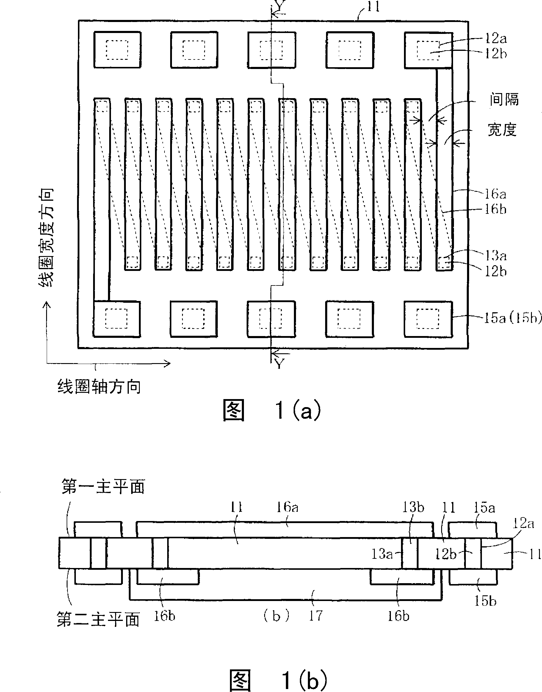
[0077] Figures 1(a) and 1(b) show the basic parts of a micro power converter according to the first embodiment (Example 1) of the present invention, wherein Figure 1(a) is viewed from the first main plane (front) side View the plane view of the thin film magnetic induction element, and Fig. 1(b) is a cross-sectional view taken along the line Y-Y in Fig. 1(a). Although the micro power converter includes an IC chip and other components as shown in FIG. 11 , FIGS. 1( a ) and 1 ( b ) only show thin film magnetic induction elements, and those components are omitted.
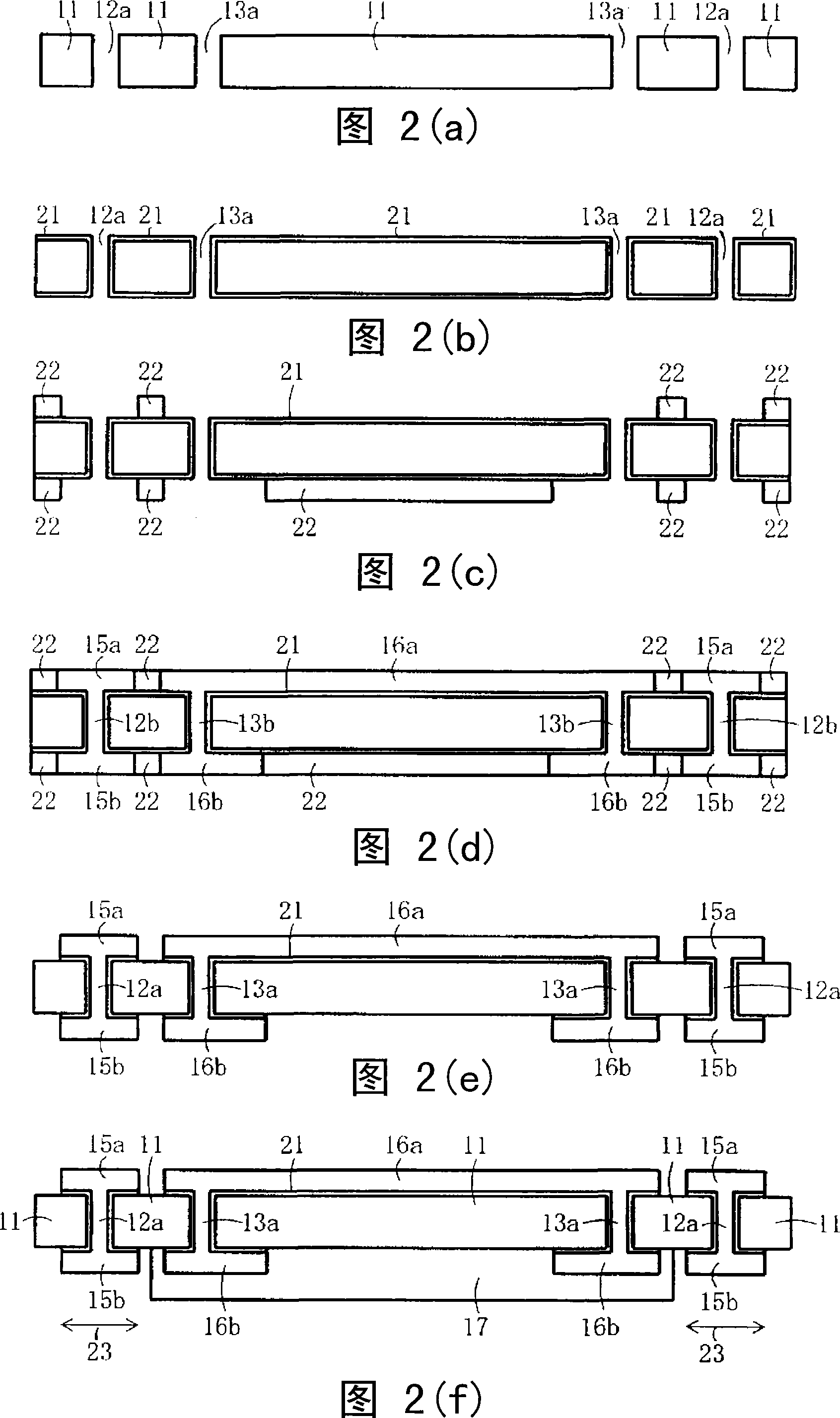
[0078] The thin-film magnetic induction element comprises: a ferrite substrate 11, which is a magnetic insulating substrate; a solenoidal coil, formed in the inner region of the ferrite substrate 11; electrode pairs, arranged between the ferrite substrate 11 and the coil in the peripheral side region in the direction parallel to the axis, where each pair of electrodes 15 a and 15 b sandwich the ferrite substrate 11 ag...
example 2
[0104] Figure 5(a) and 5(b) show the structure of the basic part of the micro power converter according to the second embodiment (example 2) of the present invention, wherein Figure 5(a) is viewed from the first main plane side The plane view of the thin film magnetic induction element, and Fig. 5(b) is a cross-sectional view taken along line A-A in Fig. 5(a).
[0105] In this embodiment, a gap 50 having a configuration of passing through the slit of the ferrite substrate 11 is formed to extend from the via hole 12a connecting the electrode 15a on the first main plane with the electrode 15b on the second main plane. , and the electrodes 15a and 15b are electrically connected through the connecting conductor 12b. Providing the gap 50 with a slot configuration reduces the width of the ferrite substrate 11 outside the electrodes 15a, 15b, thereby reducing the peripheral magnetic flux 43 flowing outside the electrodes 15a, 15b. When the through hole 12a and the slit-shaped gap 50...
example 3
[0109] Fig. 7 (a) and 7 (b) have shown the basic part according to the miniature power converter of example 3 of the present invention, wherein Fig. 7 (a) is the plan view of the thin film magnetic induction element viewed from the first main plane side, and Fig. 7(b) is a sectional view taken along line A-A in Fig. 7(a).
[0110] In Example 3, the oval-shaped through hole 12a connecting the electrode 15a on the first main plane and the electrode 15b on the second main surface is different from that of Example 2 shown in FIGS. 5(a) and 5(b). The point is that the elliptical-shaped through-hole 12a extends to the outer peripheral end portion of the ferrite substrate 11, thereby forming a slit-shaped gap 60 that intercepts the outer peripheral magnetic flux 43. This slit-like gap 60 passes completely through the ferrite substrate.
[0111] Since the portion of the ferrite substrate outside the electrodes 15a, 15b is completely removed, the outer peripheral magnetic flux 43 flow...
PUM
 Abstract
Description
Claims
Application Information


