Liquid crystal display device and electronic device
Inactive Publication Date: 2008-06-12
SEMICON ENERGY LAB CO LTD
View PDF24 Cites 163 Cited by
Summary
Abstract
Description
Claims
Application Information
AI Technical Summary
This helps you quickly interpret patents by identifying the three key elements:
Problems solved by technology
Method used
Benefits of technology
Benefits of technology
[0009]As described above, a pixel electrode or a common electrode has been formed of a light-transmitting conductive film, for example, ITO. In order to manufacture a semiconductor device which controls transmissive liquid crystal molecules and a transmissive liquid crystal display device, a pixel electrode and a common electrode are needed to be formed of a light-transmitting conductive film. Conventionally, after formation of a light-transmitting conductive film, the light-transmitting conductive film has been processed to form a pixel electrode and a common electrode by etching or the like. Thus, the number of manufacturing steps and the number of masks have been increased, and manufacturing cost has been increased.
[0010]In view of the above, objects of the invention are to provide a semiconductor device, a liquid crystal display device, and an electronic device which have a wide viewing angle and in which the number of manufacturing steps and the number of masks are small and manufacturing cost is low.
[0011]In the invention, a light-transmitting conductive film is formed to use as one of a pixel electrode and a common electrode of a liquid crystal display device without processing. Thus, the light-transmitting conductive film is not needed to be processed by etching or the like, so that the number of manufacturing steps and the number of masks can be reduced and manufacturing cost can be suppressed.
Problems solved by technology
Thus, the number of manufacturing steps and the number of masks have been increased, and manufacturing cost has been increased.
Method used
Image
Click on the blue label to locate the original text in one second.
Reading with bidirectional positioning of images and text.
Examples
embodiment mode 1
[0189]This embodiment mode is described with reference to FIGS. 1 and 3 to 5.
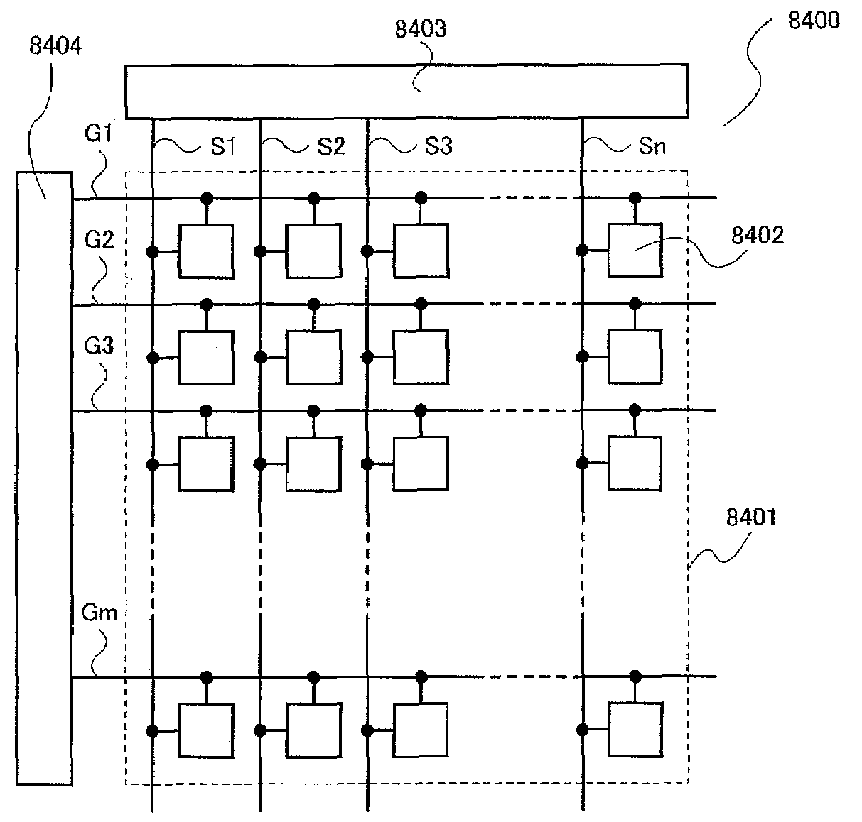
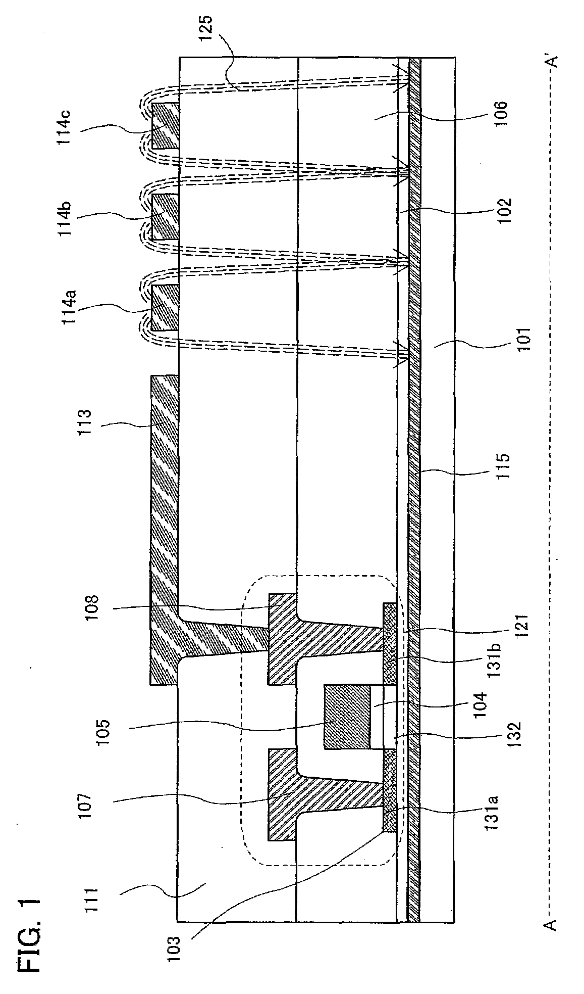
[0190]FIG. 1 shows an example where a top-gate thin film transistor (TFT) is used as a switching element in a pixel portion. A conductive film 115 to be a first electrode in FFS (Fringe-Field Switching) drive is formed over an entire surface of one side of a substrate 101.
[0191]A light-transmitting conductive film is used as the conductive film 115. As such a light-transmitting conductive film, an indiumtinoxide (ITO) film, an indiumzincoxide (IZO) film, an indiumtinoxide containing silicon (also referred to as ITSO) film, a zinc oxide (ZnO) film, a cadmiumtin oxide (CTO) film, a tin oxide (SnO) film, or the like may be used.
[0192]A base film 102 is formed over the conductive film 115, and a thin film transistor (TFT) 121 is formed over the base film 102. The TFT 121 includes a region 131a which is one of a source region and a drain region, a region 131b which is the other of the source region and th...
embodiment mode 2
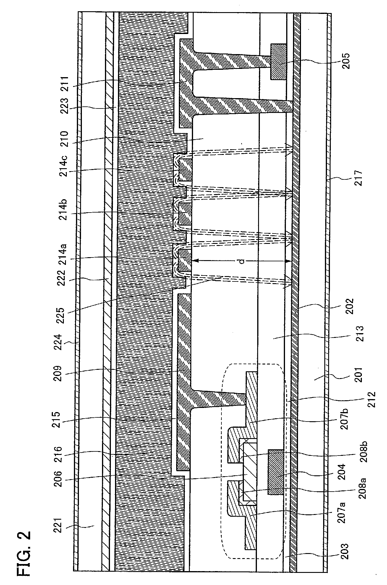
[0296]In this embodiment mode, an example in which a bottom-gate TFT is formed as a switching element in a pixel portion is described with reference to FIG. 2.
[0297]A conductive film 202, a base film 203, a gate electrode 204, a gate insulating film 213, an island-shaped semiconductor film 206 to be an active layer, a region 208a which is one of a source region and a drain region, a region 208b which is the other of the source region and the drain region, an electrode 207a which is one of a source electrode and a drain electrode, an electrode 207b which is the other of the source electrode and the drain electrode, and pixel electrodes 209 and 214 (214a, 214b, 214c, and the like) are formed over a substrate 201. A TFT 212 includes the gate electrode 204, the gate insulating film 213, the island-shaped semiconductor film 206, and the regions 208a and 208b.
[0298]A horizontal electric field 225 is generated between the pixel electrodes 214 and the conductive film 202. Liquid crystal mo...
embodiment mode 3
[0319]In this embodiment mode, FIG. 6 shows an example where the electrode 108 in Embodiment Mode 1 is not formed and the pixel electrode 113 is formed to be directly connected to the region 131b. The reference numerals in Embodiment Mode 1 are used for reference numerals in FIG. 6. Materials and manufacturing steps of the other structures can refer to those described in Embodiment Mode 1. This embodiment mode has an advantage of improvement in aperture ratio because the electrode 108 is not formed.
[0320]A bottom-gate TFT described in Embodiment Mode 2 may be used when needed.
[0321]According to this embodiment mode, a liquid crystal display device with a wide viewing angle and lower manufacturing cost than a conventional liquid crystal display device can be provided.
[0322]In the invention, since a conductive film is formed over an entire surface of a substrate, an impurity from the substrate can be prevented from being mixed into an active layer. Thus, a semiconductor device with hi...
PUM
Abstract
To provide a semiconductor device, a liquid crystaldisplay device, and an electronic device which have a wide viewing angle and in which the number of manufacturing steps, the number of masks, and manufacturing cost are reduced compared with a conventional one. The liquid crystaldisplay device includes a first electrode formed over an entire surface of one side of a substrate; a first insulating film formed over the first electrode; a thin film transistor formed over the first insulating film; a second insulating film formed over the thin film transistor; a second electrode formed over the second insulating film and having a plurality of openings; and a liquid crystal over the second electrode. The liquid crystal is controlled by an electric field between the first electrode and the second electrode.
Description
BACKGROUND OF THE INVENTION[0001]1. Field of the Invention[0002]The present invention relates to a semiconductor device and a liquid crystal display device. In particular, the present invention relates to a semiconductor device and a liquid crystal display device in which liquid crystal molecules are controlled by generating an electric field having a component parallel to a substrate.[0003]2. Description of the Related Art[0004]One of technical development strategies of a liquid crystal display device is to widen a viewing angle. As a technique for realizing a wide viewing angle, a method is used in which a gray scale is controlled by generating an electric field parallel (i.e., in a lateral direction) to a substrate to move liquid crystal molecules in a plane parallel to the substrate.[0005]Examples of such a method include an IPS (In-Plane Switching) mode and an FFS (Fringe-Field Switching) mode.[0006]In an IPS mode liquid crystal display device, two comb-shaped electrodes (also ...
Claims
Application Information
Patent Timeline
Application Date:The date an application was filed.
Publication Date:The date a patent or application was officially published.
First Publication Date:The earliest publication date of a patent with the same application number.
Issue Date:Publication date of the patent grant document.
PCT Entry Date:The Entry date of PCT National Phase.
Estimated Expiry Date:The statutory expiry date of a patent right according to the Patent Law, and it is the longest term of protection that the patent right can achieve without the termination of the patent right due to other reasons(Term extension factor has been taken into account ).
Invalid Date:Actual expiry date is based on effective date or publication date of legal transaction data of invalid patent.

