Method of manufacturing driving-device for unit pixel of organic light emitting display

a technology of organic light emitting display and driving device, which is applied in the direction of basic electric elements, semiconductor devices, electrical apparatus, etc., can solve the problems of complex manufacturing process, high manufacturing cost, and limited brightness, and achieve the effect of improving manufacturing process and simplifying process

Active Publication Date: 2008-06-26
SAMSUNG ELECTRONICS CO LTD
View PDF3 Cites 20 Cited by
  • Summary
  • Abstract
  • Description
  • Claims
  • Application Information

AI Technical Summary

Benefits of technology

[0009]The present invention provides a method of manufacturing a driving-device for a unit pixel of an organic light emitting display having

Problems solved by technology

However, since LCDs are light-receiving type displays, there are technical restrictions in brightness, contrast, view angle, and large size or the like.
Thus, there are problems that manufacturing costs increase and manufacturing processes are complicated.
Meanwhile, when an amorphous silicon TFT is simultaneously used as a switching TFT and a driving TFT, the amorph

Method used


Image

  • Method of manufacturing driving-device for unit pixel of organic light emitting display
  • Method of manufacturing driving-device for unit pixel of organic light emitting display
  • Method of manufacturing driving-device for unit pixel of organic light emitting display

Examples


Embodiment Construction

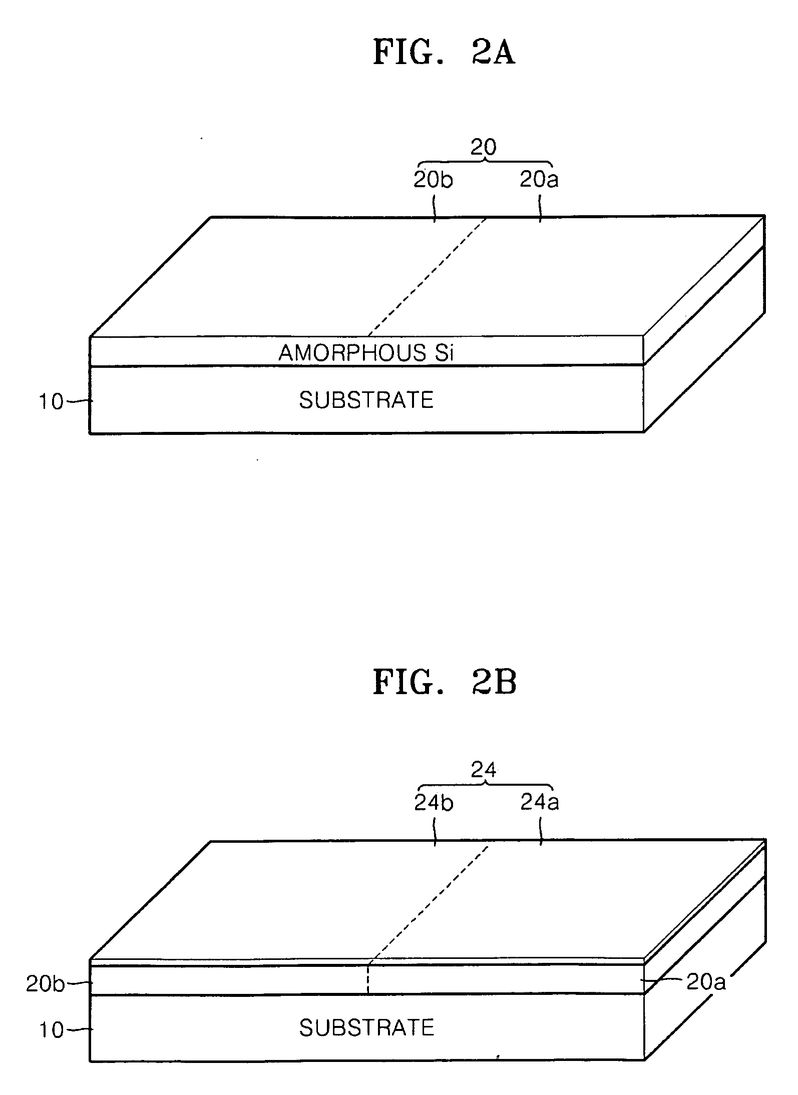
[0019]The present invention will now be described more fully with reference to the accompanying drawings, in which exemplary embodiments of the invention are shown. In the drawings, the thicknesses of layers and regions are exaggerated for clarity.

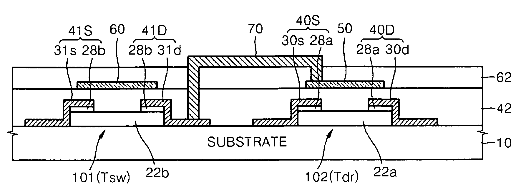
[0020]FIG. 1 is a schematic cross-sectional view of a driving device for a unit pixel of an organic light emitting display according to an embodiment of the present invention.

[0021]Referring to FIG. 1, according to an embodiment of the present invention, a driving device for a unit pixel of an organic light emitting display including a pair of a switching thin film transistor (TFT)(Tsw) 101 and a driving TFT(Tdr) 102, which are electrically connected to each other, is formed on a substrate 10.

[0022]The driving TFT 102 includes a first channel region 22a and a first gate electrode 50, which is formed on the first channel region 22a and faces the first channel region 22a. The driving TFT 102 is formed in a top gate structure, as illustrated ...


PUM


Abstract

Provided is a method of manufacturing a driving-device for a unit pixel of an organic light emitting display having an improved manufacturing process in which the driving device can be manufactured with a smaller number of processes and in simpler processes. The method includes: forming an amorphous silicon layer including a first amorphous region and a second amorphous region disposed on the same plane of a substrate; forming an SAM (self-assembled monolayer) having a hydrophobic property on the first amorphous region; coating an aqueous solution in which nickel particles are dispersed, on the second amorphous region and the SAM, wherein a larger amount of nickel particles than on the SAM are dispersed on the second amorphous region using a hydrophilicity difference between the second amorphous region and the SAM; vaporizing the SAM through an annealing process and simultaneously performing metal induced crystallization in which the nanoparticles are used as a medium, to crystallize the first and second amorphous regions and to form first and second crystallization regions; patterning the first and second crystallization regions to form first and second channel regions; and forming first and second electrodes on the first and second channel regions.

Description

CROSS-REFERENCE TO RELATED PATENT APPLICATIONS[0001]This application claims the benefit of Korean Patent Application No. 10-2006-0133094, filed on Dec. 22, 2006, in the Korean Intellectual Property Office, the disclosure of which is incorporated herein in its entirety by reference.BACKGROUND OF THE INVENTION[0002]1. Field of the Invention[0003]The present invention relates to a method of manufacturing a driving-device for a unit pixel of an organic light emitting display, and more particularly, to a method of manufacturing a driving-device for a unit pixel of an organic light emitting display having an improved manufacturing process in which the driving device can be manufactured with a smaller number of processes and in simpler processes.[0004]2. Description of the Related Art[0005]Liquid crystal displays (LCDs) which are light and have low power consumption, have been most noticed in the field of flat panel displays (FPDs). However, since LCDs are light-receiving type displays, th...

Claims


Application Information

Patent Timeline
IPC IPC(8): H01L21/336
CPCH01L21/02532H01L21/02595H01L27/3262H01L27/1229H01L27/1277H01L21/02672H10K59/1213
Inventor JUNG, JI-SIMHAHN, JUNG-SEOKLEE, SANG-YOONKIM, JONG-MANKWON, JANG-YEONPARK, KYUNG-BAE
Owner SAMSUNG ELECTRONICS CO LTD
Why Eureka
Try Eureka