Organic thin film transistor and method for manufacturing the same

a thin film transistor and organic technology, applied in the field of thin film transistors, can solve the problems of undesirable adhesion among the material layers disclosed in the reference, increased manufacturing costs, acid or base solution harming the material layer, etc., and achieves the effect of improving the adhesion among the film layers and boosting the performance of the devi

Active Publication Date: 2008-07-03
WUHAN CHINA STAR OPTOELECTRONICS TECH CO LTD
View PDF14 Cites 25 Cited by
  • Summary
  • Abstract
  • Description
  • Claims
  • Application Information

AI Technical Summary

Benefits of technology

[0010]In view of the foregoing, the present invention provides an OTFT to

Problems solved by technology

Thereby, the manufacturing costs are increased, and the acid or base solution does harm to material layers such as the organic semiconductor layers during the photolithography process.
However, adhesion among the material laye

Method used


Image

  • Organic thin film transistor and method for manufacturing the same
  • Organic thin film transistor and method for manufacturing the same
  • Organic thin film transistor and method for manufacturing the same

Examples


Embodiment Construction

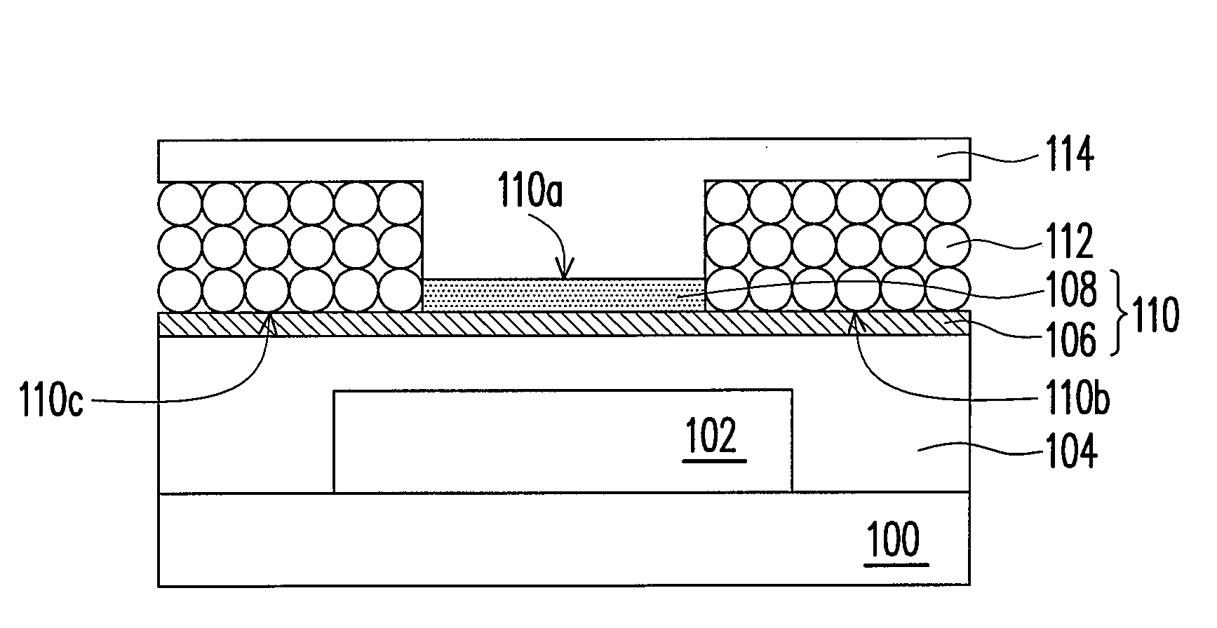
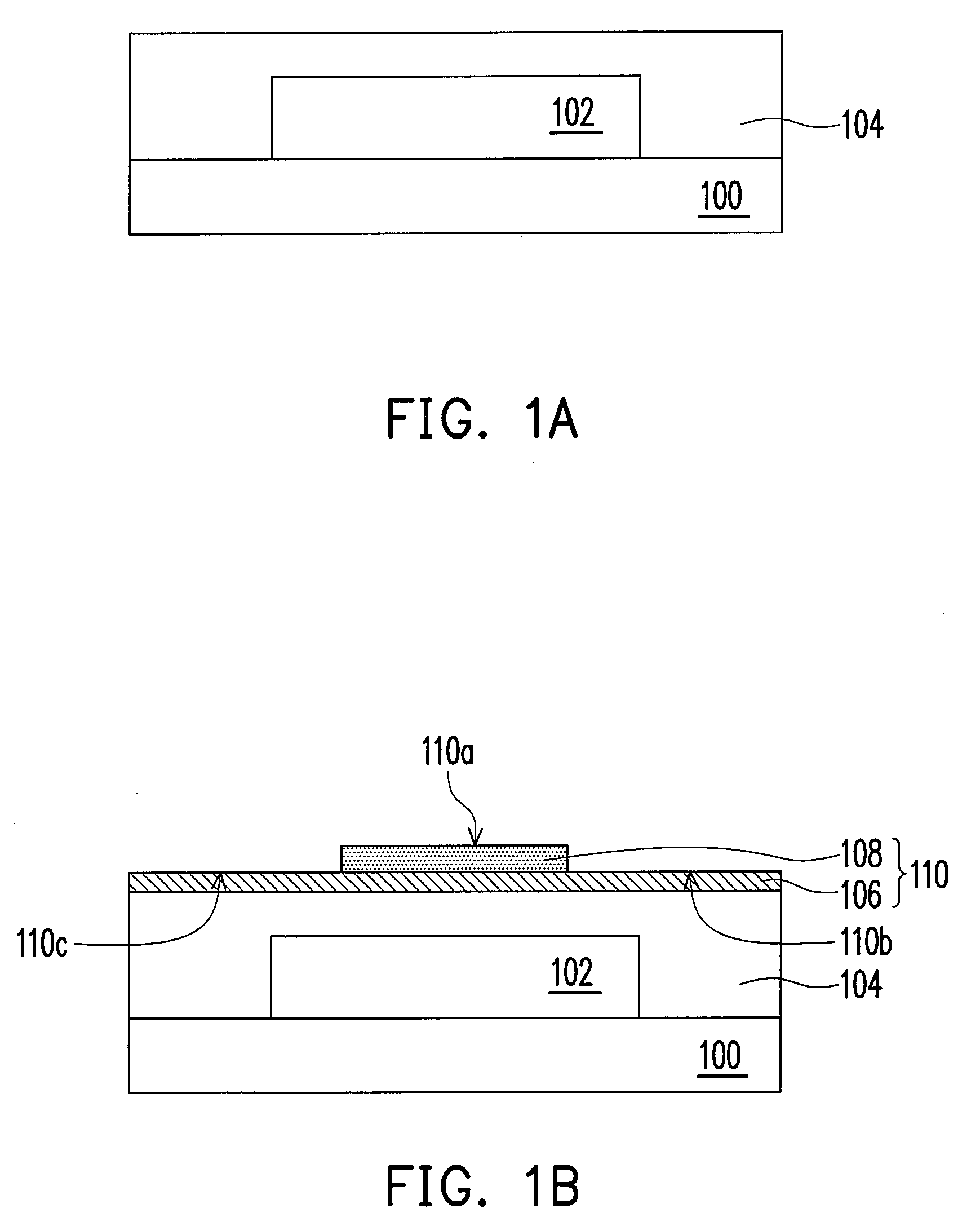
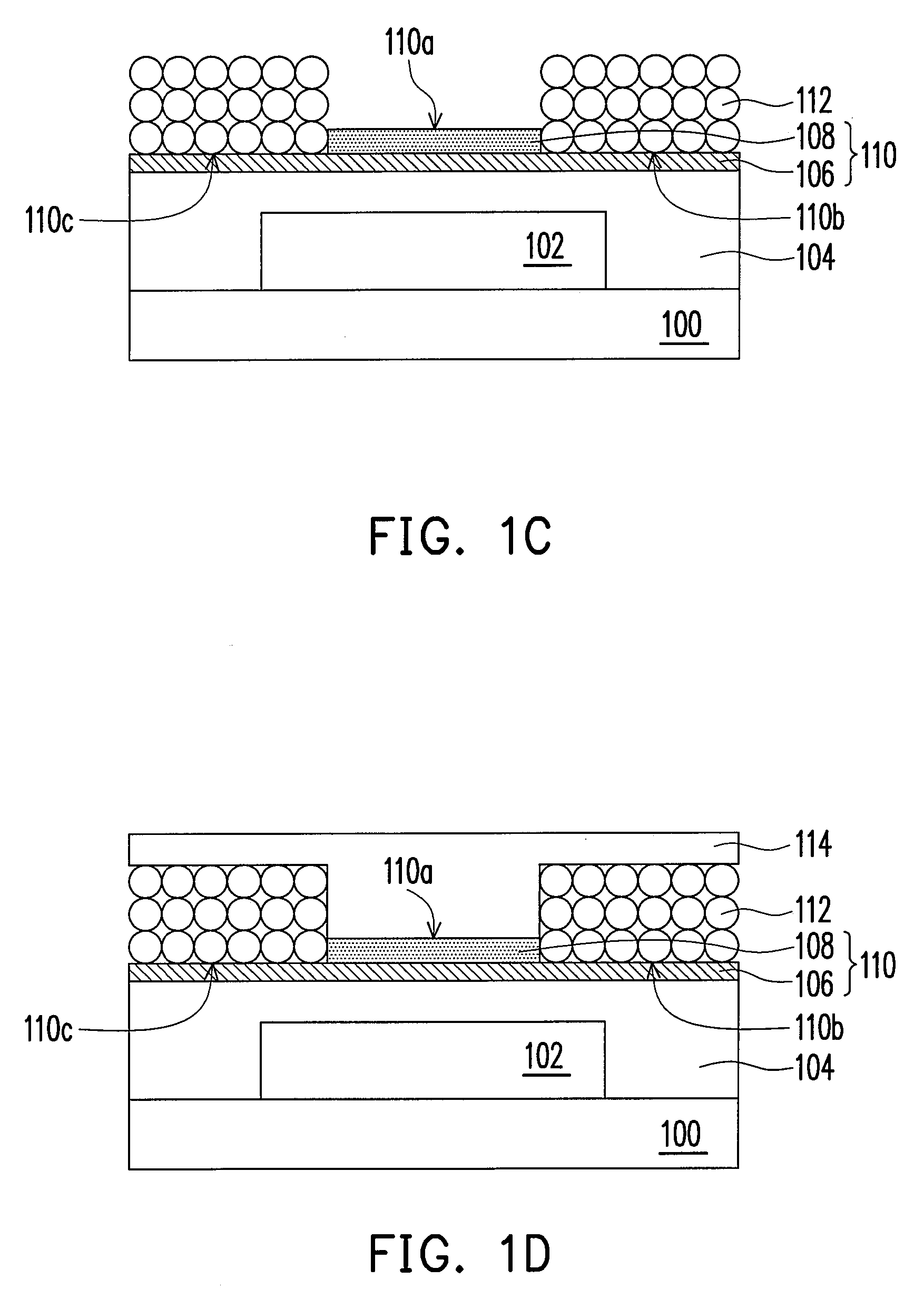
[0034]FIGS. 1A through 1D are cross-sectional views illustrating the steps of manufacturing an OTFT according to an embodiment of the present invention.

[0035]Referring to FIG. 1A, a substrate 100 is provided. The substrate 100 is, for example, a plastic substrate or a glass substrate. Next, a gate 102 is formed on the substrate 100. The material of the gate 102 includes, for example, chromium (Cr), aluminum (Al), aluminum neodymium (AlNd), other appropriate metals, or an alloy of metals. The method for forming the gate 102 includes, for example, performing a CVD process or a PVD process. It is certain that the material of the gate 102 can be, for example, Au nano-particles, Ag nano-particles, Pd nano-particles, Cu nano-particles or other appropriate metal nano-particles, and the method of forming the gate 102 includes, for example, performing a transfer printing process or an ink-jet process.

[0036]Again, referring to FIG. 1A, a gate insulator 104 is formed to cover the gate 102 and ...


PUM


Abstract

An organic thin film transistor including a substrate, a gate, a gate insulator, an adhesive layer, a metal nano-particle layer and an organic semiconductor layer is provided. The gate is disposed on the substrate. The gate insulator is disposed on the gate and the substrate. The adhesive layer is disposed on the gate insulator. Besides, the adhesive layer has a hydrophobic surface above the gate and a first hydrophilic surface and a second hydrophilic surface on two sides of the hydrophobic surface. A surface of the metal nano-particle layer is modified by a hydrophilic group, and the metal nano-particle layer is disposed on the first and the second hydrophilic surfaces of the adhesive layer as a source and a drain, respectively. The organic semiconductor layer is disposed on the hydrophobic surface of the adhesive layer and on the metal nano-particle layer.

Description

CROSS-REFERENCE TO RELATED APPLICATION[0001]This application claims the priority benefit of Taiwan application serial no. 96100086, filed on Jan. 2, 2007. All disclosure of the Taiwan application is incorporated herein by reference.BACKGROUND OF THE INVENTION[0002]1. Field of the Invention[0003]The present invention generally relates to a thin film transistor (TFT) and a method of manufacturing the same, and more particularly to an organic thin film transistor (OTFT) and a method of manufacturing the same.[0004]2. Description of Related Art[0005]The principles of operating a TFT are similar to those of operating a conventional metallic-oxide-semiconductor (MOS) transistor. Both the TFT and the MOS transistor have three terminals (a gate, a drain and a source). Each TFT functions as a switching element inside a liquid crystal display (LCD) pixel unit.[0006]Currently, an organic thin film transistor (OTFT) has been developed in the industry. In comparison with the conventional TFT, th...

Claims


Application Information

Patent Timeline
IPC IPC(8): H01L51/30H01L51/40
CPCH01L51/0022H01L51/102H01L51/0545H01L51/0529
Inventor TSAI, YI-YUNWU, CHUAN-YILAI, CHIN-CHUAN
Owner WUHAN CHINA STAR OPTOELECTRONICS TECH CO LTD
Why Eureka
Try Eureka