RF module package

a module package and module technology, applied in the direction of semiconductor devices, semiconductor/solid-state device details, electrical apparatus, etc., can solve the problems of time-consuming manufacturing process, inability to meet the demand of producing smaller chips with high-density elements on the chip, and inability to meet the demand of producing smaller chips. , to achieve the effect of excellent thermal dissipation, shrinkage size, and cte performan

Active Publication Date: 2008-07-03
ADL ENERGY CORP
View PDF11 Cites 87 Cited by
  • Summary
  • Abstract
  • Description
  • Claims
  • Application Information

AI Technical Summary

Benefits of technology

[0006]The object of the present invention is to provide RF module package with excellent thermal dissipation, CTE performance and shrinkage size.

Problems solved by technology

As a semiconductor become more complicated, the traditional package technique, for example lead frame package, flex package, rigid package technique, can't meet the demand of producing smaller chip with high density elements on the chip.
Furthermore, because conventional package technologies have to divide a dice on a wafer into respective dies and then package the die respectively, therefore, these techniques are time consuming for manufacturing process.
Since the chip package technique is highly influenced by the development of integrated circuits, therefore, as the size of electronics has become demanding, so does the package technique.
However, the prior RF module package employs LTCC (low-temperature co-fired ceramic) and the disadvantage is listed as follows; Low On Board Reliability (TCT—temperature cycling test); Need extra metal plate for heat dissipation, Long manufacturing cycle; Higher manufacturing cost; IC need to be packaged in advance; Still need wire bonding or SMT (surface mount technology) process; Thick package body (˜1.4 mm).

Method used


Image

  • RF module package
  • RF module package
  • RF module package

Examples


Embodiment Construction

[0015]The invention will now be described in greater detail with preferred embodiments of the invention and illustrations attached. Nevertheless, it should be recognized that the preferred embodiments of the invention is only for illustrating. Besides the preferred embodiment mentioned here, present invention can be practiced in a wide range of other embodiments besides those explicitly described, and the scope of the present invention is expressly not limited expect as specified in the accompanying Claims.

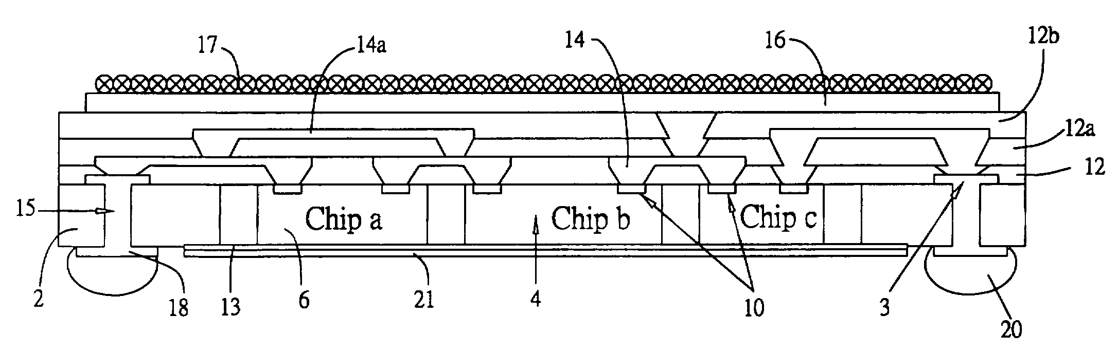
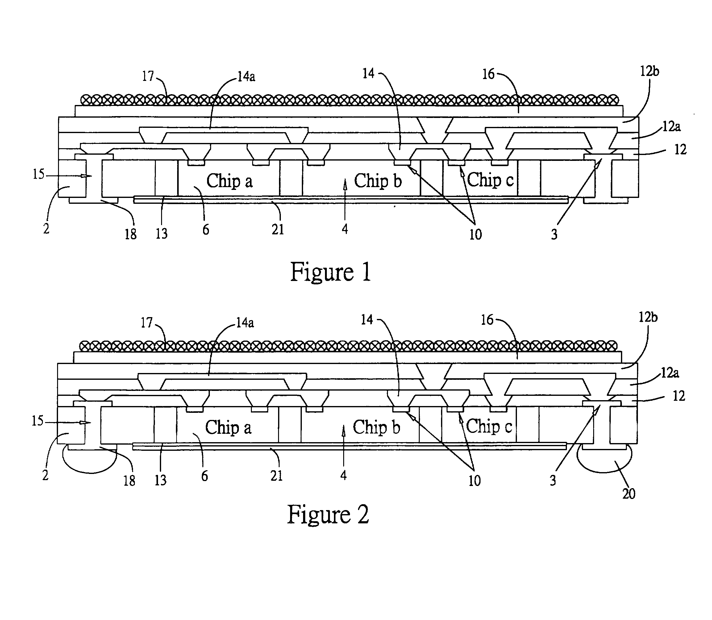
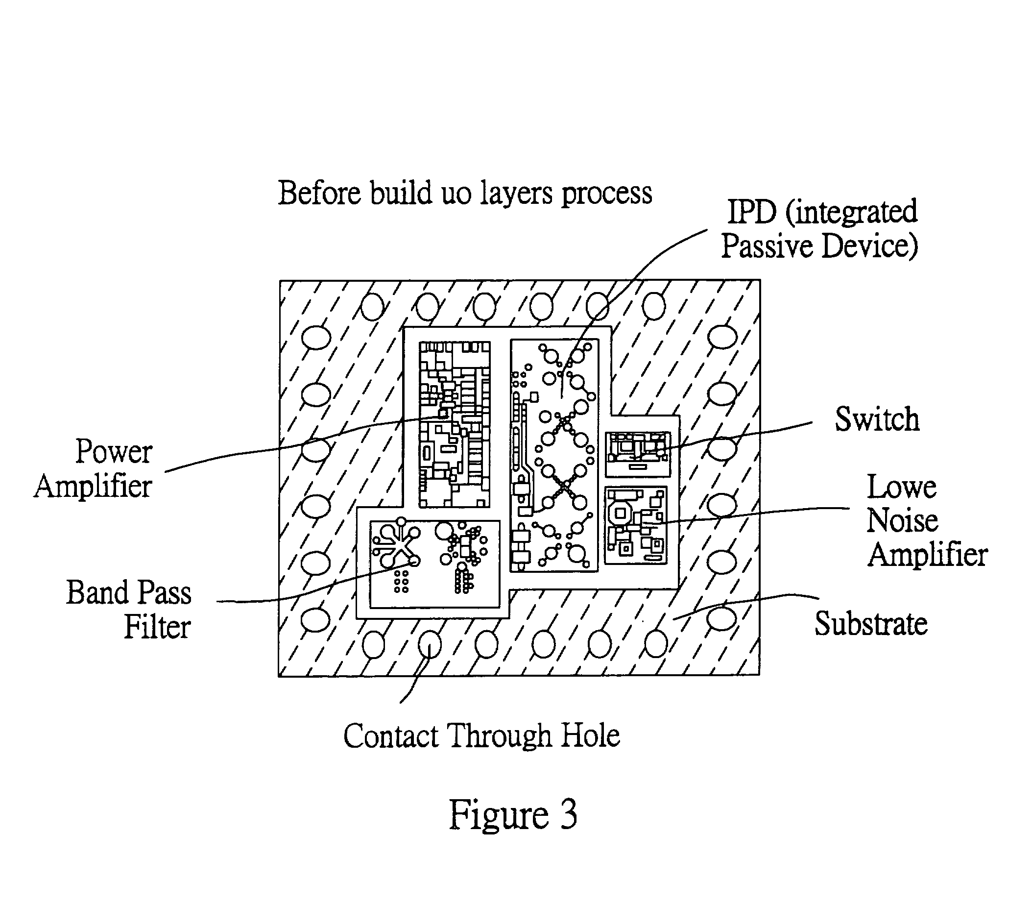
[0016]The present invention discloses a structure of RF module package utilizing a substrate having predetermined terminal contact metal pads 3 and metal through holes 15 formed thereon and a pre-formed die receiving through holes 4 formed into the substrate 2. A multi-dice 6 are (chip a, chip b and chip n) disposed within the die receiving through hole of the substrate, an elastic core paste material is filled into the space between dice, die edge and side wall of die receiving t...


PUM

PropertyMeasurementUnit
diameteraaaaaaaaaa
diameteraaaaaaaaaa
elongation rateaaaaaaaaaa

Abstract

The present invention discloses a structure of package comprising: a substrate with a die receiving through hole; a base attached on a lower surface of the substrate; a die disposed within the die receiving through hole and attached on the base; a dielectric layer formed on the die and the substrate; a re-distribution layer (RDL) formed on the dielectric layer and coupled to the die; a protection layer formed over the RDL; and pluralities of pads formed on the protection layer and coupled to the RDL. The RDL is made from an alloy comprising Ti / Cu / Au alloy or Ti / Cu / Ni / Au alloy.

Description

FIELD OF THE INVENTION[0001]This invention relates to a structure of package, and more particularly to a RF (radio frequency) module package with die receiving through-hole of substrate to improve the reliability and to reduce the device size.DESCRIPTION OF THE PRIOR ART[0002]In the field of semiconductor devices, the device density is increased and the device dimension is reduced, continuously. The demand for the packaging or interconnecting techniques in such high density devices is also increased to fit the situation mentioned above. Conventionally, in the flip-chip attachment method, an array of solder bumps is formed on the surface of the die. The formation of the solder bumps may be carried out by using a solder composite material through a solder mask for producing a desired pattern of solder bumps. The function of chip package includes power distribution, signal distribution, heat dissipation, protection and support . . . and so on. As a semiconductor become more complicated...

Claims


Application Information

Patent Timeline
Patent Type & Authority Applications(United States)
IPC IPC(8): H01L23/485H01L21/60
CPCH01L23/467H01L2224/32245H01L23/66H01L24/24H01L24/82H01L25/16H01L2224/24137H01L2924/01015H01L2924/01027H01L2924/01029H01L2924/01033H01L2924/01047H01L2924/01059H01L2924/01074H01L2924/01075H01L2924/01078H01L2924/01079H01L2924/01082H01L2924/09701H01L2924/10329H01L2924/14H01L2924/15311H01L2924/19011H01L2924/19041H01L2924/19042H01L2924/19043H01L2924/30105H01L2924/3025H01L2924/01005H01L2924/01006H01L2924/01019H01L2924/01068H01L2924/01087H01L2924/014H01L2224/73267H01L2924/10253H01L23/5389H01L2924/00H01L2924/351H01L23/12
Inventor YANG, WEN-KUNYU, CHUN-HUILIN, CHIHWEI
Owner ADL ENERGY CORP
Why Eureka
Try Eureka