Method and System for Model-Based Routing of an Integrated Circuit

a model-based routing and integrated circuit technology, applied in the field of model-based routing of integrated circuits, can solve the problems of significant thickness variation of processing films, variation of plated surface based on cmp and plating process, and large variation of post-cmp film thickness, so as to minimize the variation in surface topography, reduce the variation in deposited copper thickness, and minimize the variation in post-cmp film thickness large-range

Active Publication Date: 2008-07-03
CADENCE DESIGN SYST INC
View PDF40 Cites 48 Cited by
  • Summary
  • Abstract
  • Description
  • Claims
  • Application Information

AI Technical Summary

Benefits of technology

[0010]Variations in feature density, widths, and heights may also occur during the CMP and plating processes. Variations based upon CMP and plating process are often caused by oxide loss, dishing, erosion, or other copper losses. For ECD, the goal is to completely fill an etched trench region in a void-free manner while minimizing a variation in the deposited copper thickness and minimizing a variation in surface topography. There may exist pattern-dependencies in ECD that result in plated surface variation. Film thickness variation in CMP processes can be separated into various components: lot-to-lot, wafer-to-wafer, wafer-level, and die-level. Often, the most significant component is the pattern dependent die-level component. Die-level film thic

Problems solved by technology

However pattern dependencies between the process by which the ICs are fabricated and the pattern that is being created often cause processed films to have significant variation in thickness across a surface, resulting in variation in feature dimensions (e.g. line widths) of ICs that are patterned using the mask.
Variations based upon CMP and plating process are often caused by oxide loss, dishing, erosion, or other copper losses.
There may exist pattern-dependencies in ECD that result in plated surface variation.
As successive non-conformal layers are deposited and polished, the variation becomes worse.
The variations may lead to numerous problems and flaws in a manufactured IC, such as timing failures, decreased performance, and increased power consumption.
As just one example, because interconnect lines and connections on higher layers carry power to portions of the chip, the variations can increase the sheet resistance and thus affect the

Method used


Image

  • Method and System for Model-Based Routing of an Integrated Circuit
  • Method and System for Model-Based Routing of an Integrated Circuit
  • Method and System for Model-Based Routing of an Integrated Circuit

Examples


Embodiment Construction

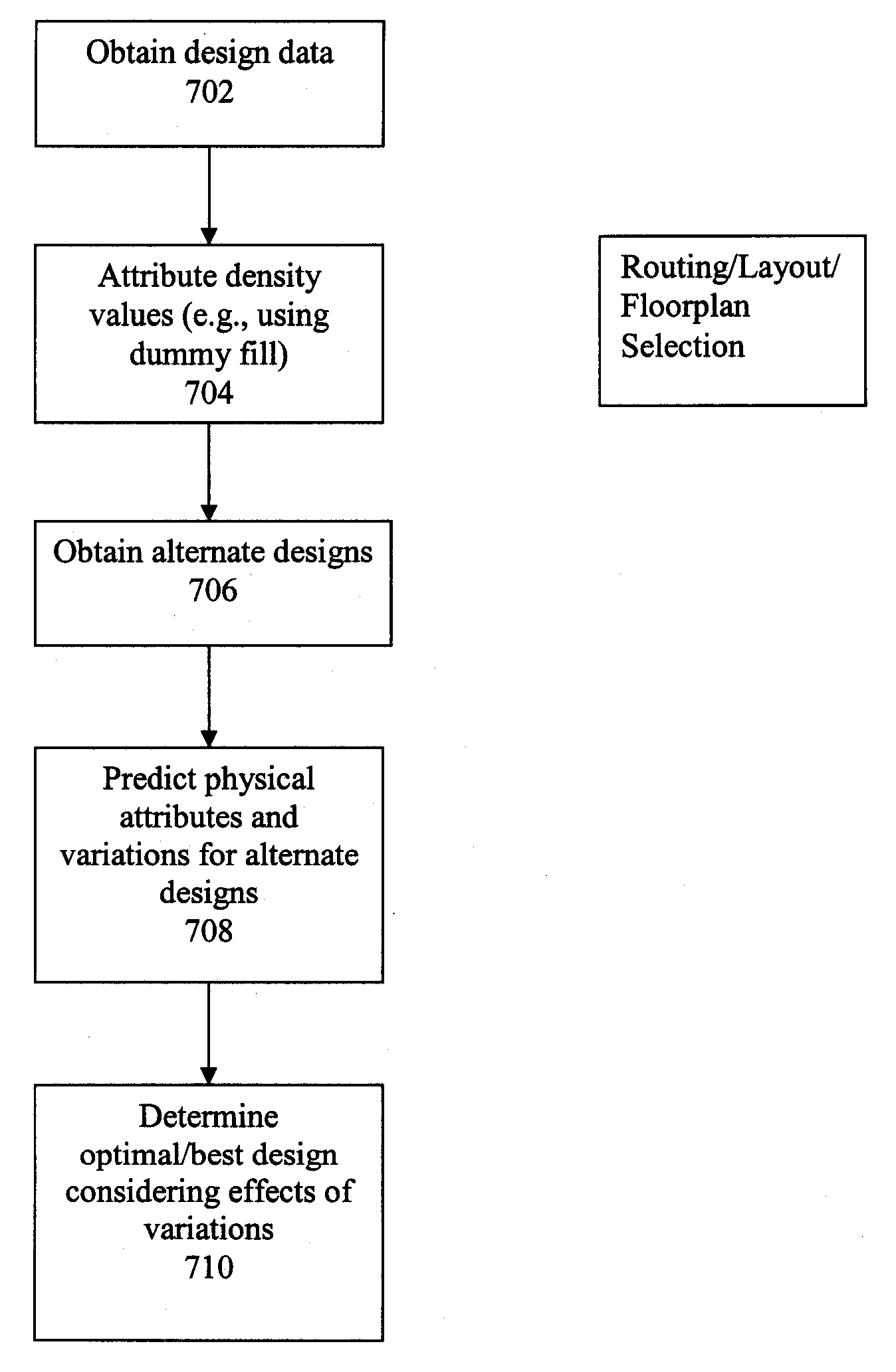
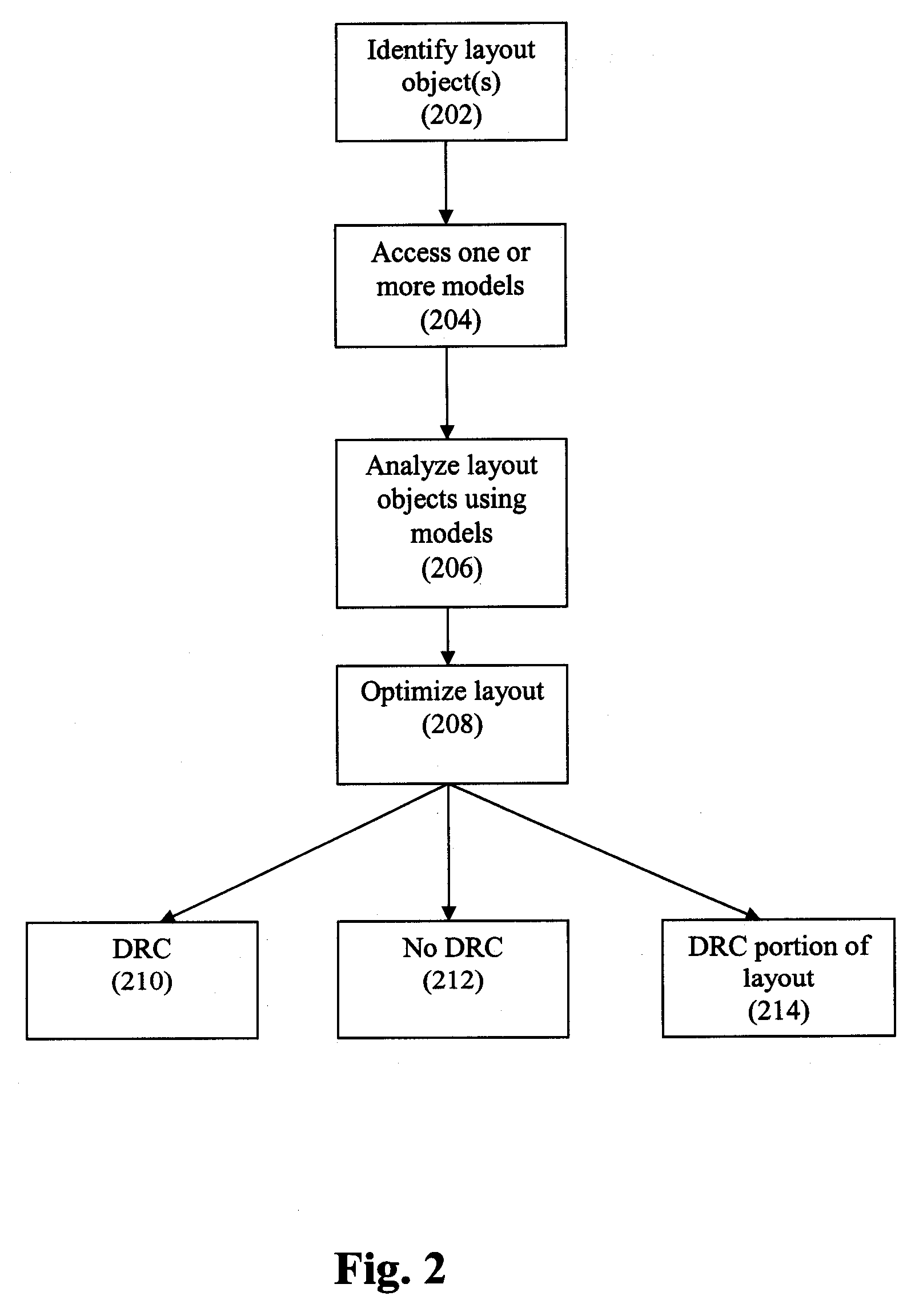
[0027]The present approach is directed to a model-based method for floorplanning, layout, placement and routing. As used herein, the term “Model” refers to a set of data that identifies one or more specific characteristics within an IC layout and data relating to its effect, manufacturability, and / or usability. For example, a model may present a defined characteristic such as “spacing” and a chart or numeric data indicating the probability of failure / success at different spacing values.

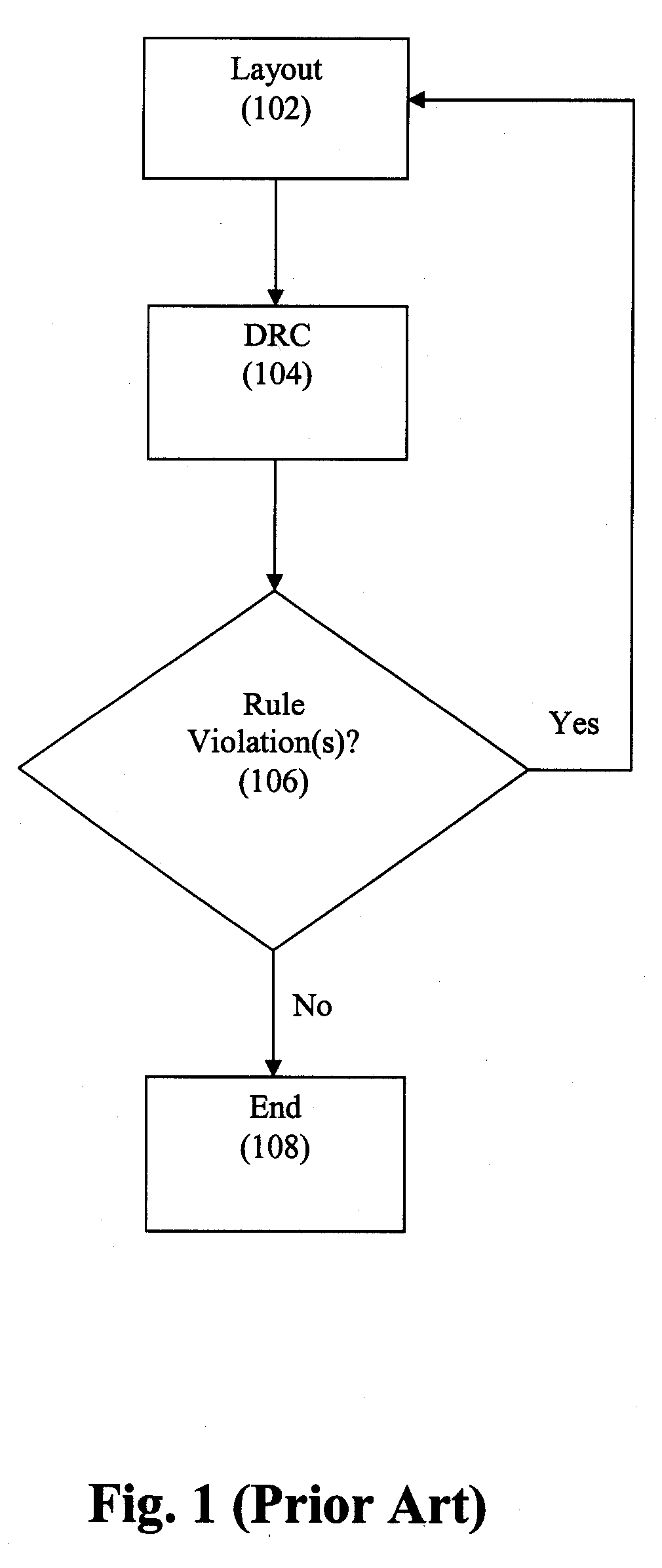
[0028]FIG. 1 shows a flowchart of a conventional process for performing electronic design using conventional non-model approaches. Conventionally, Physical Verification (PV) is one of the final steps that is performed before releasing an IC design to manufacturing. A key component of conventional PV includes the process of Design Rule Check (DRC) to ensure that the design abides by all of the detailed rules and parameters that the foundry specifies for its manufacturing process. Violating a single fou...


PUM


Abstract

Disclosed is a method, system, and computer program product for implementing model-based floorplanning, layout, placement, and routing. Models are used to guide the placement and routing of polygons on the IC layout based upon predictions of manufacturing variations.

Description

CROSS-REFERENCE TO RELATED APPLICATIONS[0001]The invention is a continuation-in-part of U.S. application Ser. No. 11 / 648,150, filed on Dec. 29, 2006, which is hereby incorporated by reference in its entirety.BACKGROUND AND SUMMARY[0002]The invention is directed to a more efficient approach for implementing floorplanning, layout, placement, and routing of integrated circuit designs.[0003]A semiconductor integrated circuit (IC) has a large number of electronic components, such as transistors, logic gates, diodes, wires, etc., that are fabricated by forming layers of different materials and of different geometric shapes on various regions of a silicon wafer.[0004]Many phases of physical design may be performed with computer aided design (CAD) tools or electronic design automation (EDA) systems. To design an integrated circuit, a designer first creates high level behavior descriptions of the IC device using a high-level hardware design language. An EDA system typically receives the high...

Claims


Application Information

Patent Timeline
IPC IPC(8): G06F17/50
CPCG06F17/5077G06F17/5072G06F30/392G06F30/394G06F30/3947
Inventor WHITE, DAVIDNEQUIST, ERIC
Owner CADENCE DESIGN SYST INC
Why Eureka
Try Eureka