Semiconductor Device

a technology of semiconductor devices and semiconductors, applied in the direction of semiconductor devices, thermoelectric device junction materials, electrical apparatus, etc., can solve the problems of data interception and data forgery, and achieve the effects of low cost, simple structure and inexpensive materials

Inactive Publication Date: 2008-07-10
SEMICON ENERGY LAB CO LTD
View PDF8 Cites 23 Cited by
  • Summary
  • Abstract
  • Description
  • Claims
  • Application Information

AI Technical Summary

Benefits of technology

[0013]In view of the foregoing, the invention provides a semiconductor device capable of communicating data wirelessly, where data can be written after the production and forgery caused by rewriting of data can be prevented. The invention also provides a semiconduc

Problems solved by technology

Since a wireless chip communicates data wirelessly, it in

Method used


Image

  • Semiconductor Device
  • Semiconductor Device
  • Semiconductor Device

Examples


embodiment mode 1

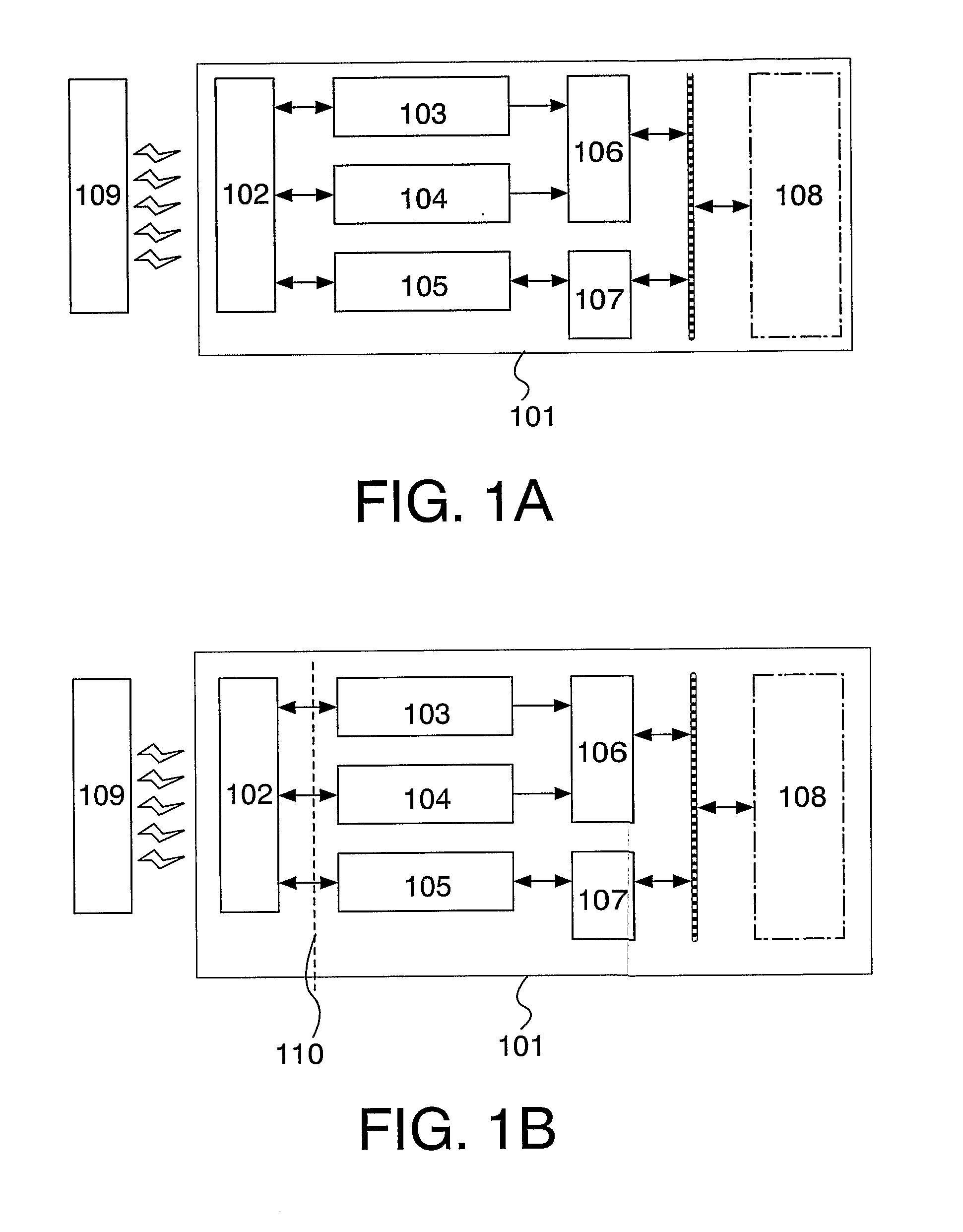
[0045]Described in this embodiment mode is a configuration of a semiconductor device of the invention, which wirelessly communicates data with an external communication device (reader / writer) through an antenna.

[0046]FIGS. 1A and 1B are schematic diagrams each showing a semiconductor device of the invention.

[0047]As shown in FIG. 1A, a semiconductor device 101 of the invention includes an antenna 102, a power supply circuit 103, a clock generation circuit 104, a demodulation / modulation circuit 105, a control circuit 106, an interface (IF) circuit 107, and a memory 108. The semiconductor device 101 can wirelessly communicate data with an external communication device (a reader / writer 109).

[0048]If the semiconductor device 101 is connected to the antenna 102 that is formed separately as shown in FIG. 1B, the semiconductor device 101 may have a wire 110 for connecting the antenna 102. If the semiconductor device 101 communicates data wirelessly, the wire 110 is connected to an antenna ...

embodiment mode 2

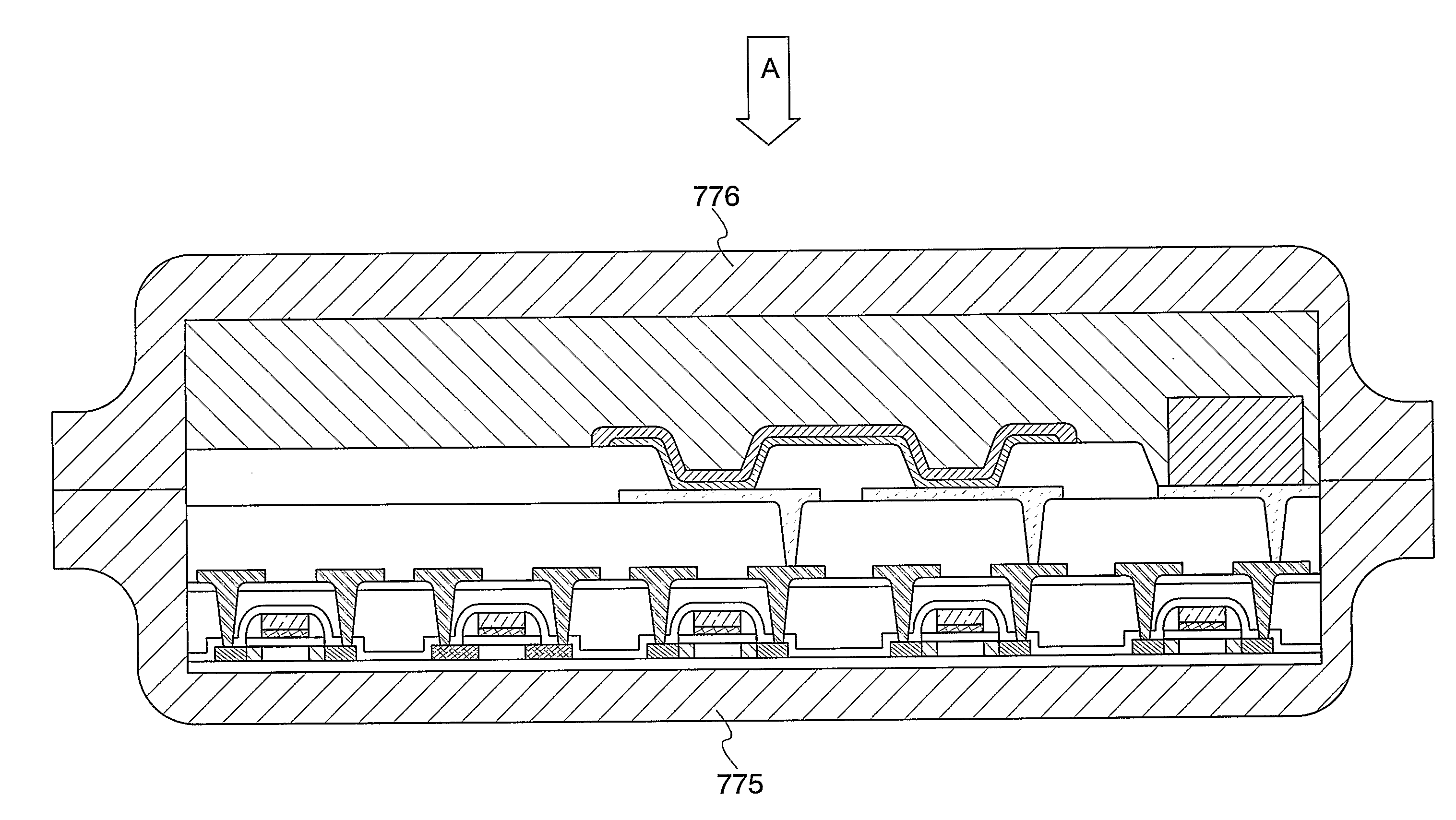
[0097]In this embodiment mode, manufacturing steps of a transistor and the memory element 208 that constitute the memory cell 206 are described with reference to FIGS. 9A to 9C, 10A 10B, 11A 11B, 12A and 12B, FIG. 3 in this order.

[0098]As the semiconductor device of the invention, a semiconductor device formed over a glass substrate may be used as it is, or a semiconductor device formed over a substrate may be separated from the substrate and attached to another flexible substrate in order to create functional added value. Described in this embodiment mode is the case of manufacturing a flexible semiconductor device by a separation process. Note that in this specification, steps of separating from a substrate and attaching to another substrate are referred to as a separation process.

[0099]First, a separation layer 503 is formed over a surface of a substrate 502 (FIG. 9A). The substrate 502 may be a glass substrate, a quartz substrate, a metal substrate or a stainless substrate havin...

embodiment mode 3

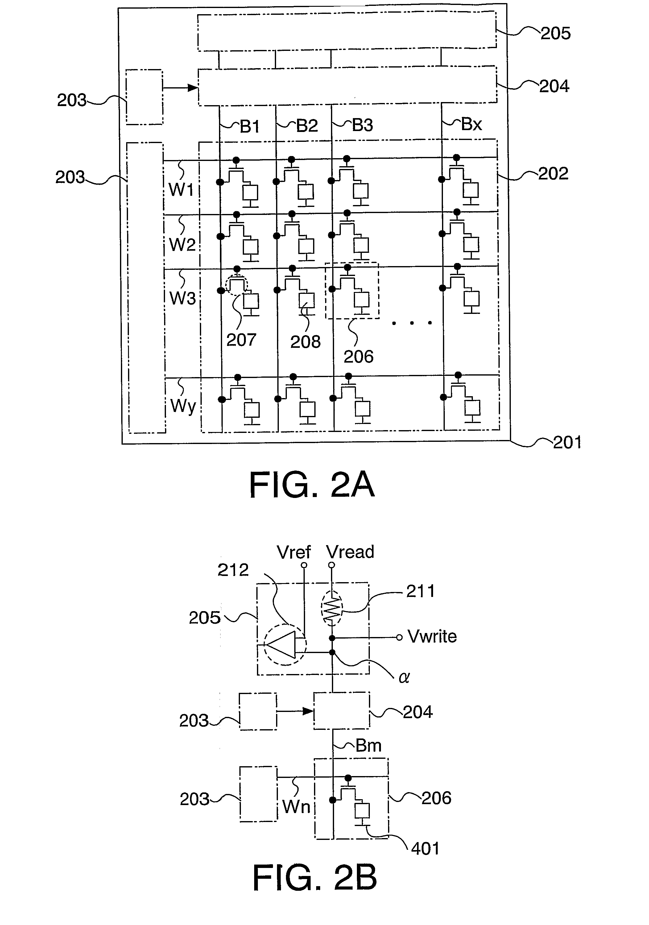
[0151]Description is made on an example where a common electrode of an organic memory included in the semiconductor device of the invention is formed in a linear shape and an example of manufacturing steps thereof. The linear shape herein means a rectangle with a second side much longer than a first side, an ellipse with a long axis, or a long shape similar to these. The common electrode is electrically connected for applying the same potential to one terminal of all memory elements. Therefore, as shown in FIGS. 5A to 5D for example, the aforementioned rectangles or ellipses are preferably formed in a comb-like pattern, which are included in the linear shape. However, the linear shape is not limited to the examples shown herein, and any of shapes that can reduce the absorption of electromagnetic waves caused by eddy currents may be adopted. Further, the common electrode 401 is only required to have a shape that can reduce the absorption of electromagnetic waves caused by eddy curren...


PUM


Abstract

The invention provides a semiconductor device where data can be written after the production and forgery caused by rewriting of data can be prevented, and which can be manufactured at a low cost using a simple structure and an inexpensive material. Further, the invention provides a semiconductor device having the aforementioned functions, where wireless communication is not blocked by the internal structure. The semiconductor device of the invention has an organic memory provided with a memory cell array including a plurality of memory cells, a control circuit for controlling the organic memory, and a wire for connecting an antenna. Each of the plurality of memory cells has a transistor and a memory element. The memory element has a structure where an organic compound layer is provided between a first conductive layer and a second conductive layer. The second conductive layer is formed in a linear shape.

Description

TECHNICAL FIELD[0001]The present invention relates to a semiconductor device capable of communicating data.BACKGROUND ART[0002]The invention relates to a semiconductor device, in particular a semiconductor device capable of communicating data wirelessly.[0003]A semiconductor device capable of communicating data wirelessly is typified by a wireless chip. A wireless chip is used for production management by assigning an identification number (ID) to an object and storing the history thereof. A wireless chip assigned an ID (wireless tag) is also used for utilization and management of personal data, money and the like. Such a wireless chip is called an ID tag, an IC card or the like, and has been manufactured in quantity and widely used with development of identification technology and increase in demand.[0004]Depending on the application, a wireless chip is changed in communication distance, communication method, size, the presence or absence of an internal power supply, configuration ...

Claims


Application Information

Patent Timeline
IPC IPC(8): H01L51/10
CPCH01L27/105H01L27/12H01L27/283H01L27/1266H01L27/13H01L27/1214H10K19/10H01L27/124
Inventor KATO, KIYOSHI
Owner SEMICON ENERGY LAB CO LTD
Why Eureka
Try Eureka