METHOD OF MANUFACTURING P-TYPE ZnO SEMICONDUCTOR LAYER USING ATOMIC LAYER DEPOSITION AND THIN FILM TRANSISTOR INCLUDING THE P-TYPE ZnO SEMICONDUCTOR LAYER

a technology of atomic layer deposition and semiconductor layer, which is applied in the direction of chemically reactive gas, crystal growth process, polycrystalline material growth, etc., can solve the problems of low reproducibility and low mobility of n- or p-doped zno layer, difficult formation of stable p-type oxide semiconductor thin layer, and low transparency of lncuoch. , to achieve the effect of simple process and excellent characteristics

Inactive Publication Date: 2008-07-10
ELECTRONICS & TELECOMM RES INST
View PDF9 Cites 30 Cited by
  • Summary
  • Abstract
  • Description
  • Claims
  • Application Information

AI Technical Summary

Benefits of technology

[0009]The present invention is directed to a method of manufacturing a low-priced p-type ZnO se

Problems solved by technology

Most research has been focused on n-type oxide semiconductor thin layers due to the fact that forming stable p-type oxide semiconductor thin layers is difficult.
The LnCuOCh has a disadvantage of low transparency, and the N- or P-doped ZnO la

Method used


Image

  • METHOD OF MANUFACTURING P-TYPE ZnO SEMICONDUCTOR LAYER USING ATOMIC LAYER DEPOSITION AND THIN FILM TRANSISTOR INCLUDING THE P-TYPE ZnO SEMICONDUCTOR LAYER
  • METHOD OF MANUFACTURING P-TYPE ZnO SEMICONDUCTOR LAYER USING ATOMIC LAYER DEPOSITION AND THIN FILM TRANSISTOR INCLUDING THE P-TYPE ZnO SEMICONDUCTOR LAYER
  • METHOD OF MANUFACTURING P-TYPE ZnO SEMICONDUCTOR LAYER USING ATOMIC LAYER DEPOSITION AND THIN FILM TRANSISTOR INCLUDING THE P-TYPE ZnO SEMICONDUCTOR LAYER

Examples


Embodiment Construction

[0027]The present invention will now be described more fully hereinafter with reference to the accompanying drawings, in which exemplary embodiments of the invention are shown.

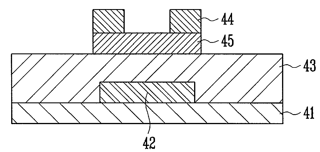
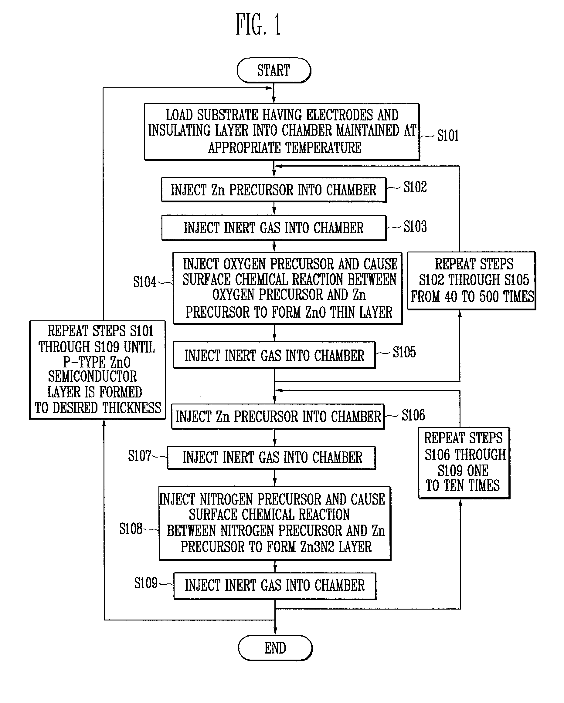
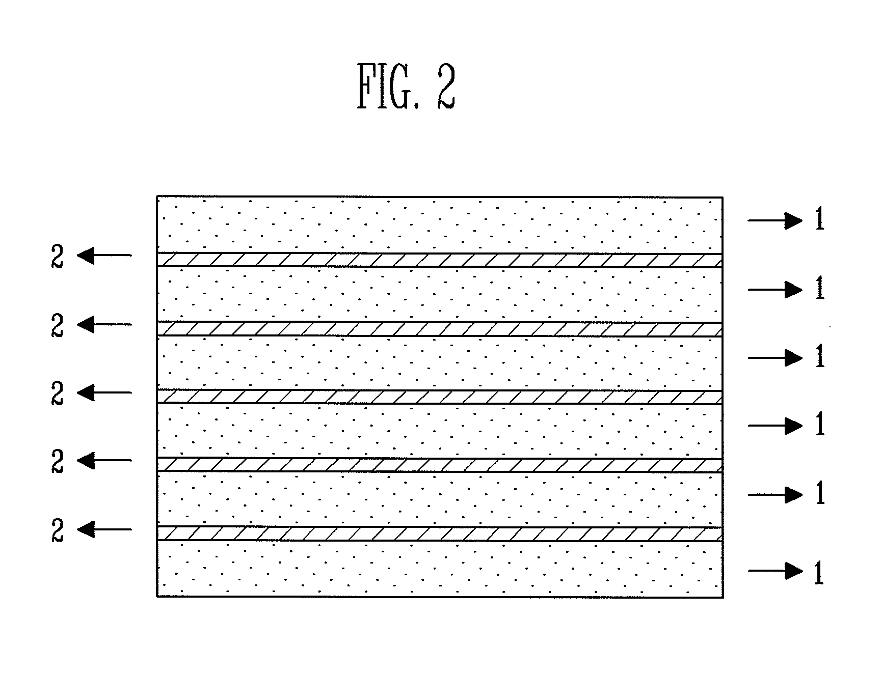
[0028]FIG. 1 is a flowchart illustrating a process of manufacturing a p-type ZnO semiconductor layer according to an exemplary embodiment of the present invention, and FIG. 2 is a cross-sectional view of a p-type ZnO semiconductor layer manufactured using the process shown in FIG. 1.

[0029]Referring to FIG. 1, in order to manufacture the p-type ZnO semiconductor layer according to the present invention, initially, a substrate is loaded into a chamber of an atomic layer deposition (ALD) apparatus in step S101. The chamber is maintained at a temperature of about 40 to 350° C., and electrodes and an insulating layer are stacked on the substrate loaded in the chamber.

[0030]In the present invention, an ALD technique includes alternating a process of chemisorbing molecules on the surface of a substrate using a chemic...


PUM

PropertyMeasurementUnit
Thicknessaaaaaaaaaa
Thicknessaaaaaaaaaa
Semiconductor propertiesaaaaaaaaaa

Abstract

Provided are a method of manufacturing a transparent N-doped p-type ZnO semiconductor layer using a surface chemical reaction between precursors containing elements constituting thin layers, and a thin film transistor (TFT) including the p-type ZnO semiconductor layer. The method includes the steps of: preparing a substrate and loading the substrate into a chamber; injecting a Zn precursor and an oxygen precursor into the chamber, and causing a surface chemical reaction between the Zn precursor and the oxygen precursor using an atomic layer deposition (ALD) technique to form a ZnO thin layer on the substrate; and injecting a Zn precursor and an nitrogen precursor into the chamber, and causing a surface chemical reaction between the Zn precursor and the nitrogen precursor to form a doping layer on the ZnO thin layer.

Description

CROSS-REFERENCE TO RELATED APPLICATION[0001]This application claims priority to and the benefit of Korean Patent Application Nos. 2007-2521, filed Jan. 9, 2007, and 2007-57097, filed Jun. 12, 2007, the disclosures of which are incorporated herein by reference in their entirety.BACKGROUND[0002]1. Field of the Invention[0003]The present invention relates to a method of manufacturing a p-type ZnO semiconductor layer using an atomic layer deposition (ALD) technique and a thin film transistor (TFT) including the p-type ZnO semiconductor layer and, more particularly, to a method of manufacturing a p-type ZnO semiconductor layer including a Zn3N2 layer or a ZnO:N layer formed through a surface chemical reaction between a Zn precursor and an nitrogen precursor on a ZnO thin layer formed through a surface chemical reaction between an oxygen precursor and a Zn precursor, and a TFT including the p-type ZnO semiconductor layer.[0004]The present invention has been produced from the work supporte...

Claims


Application Information

Patent Timeline
IPC IPC(8): H01L29/10H01L21/31
CPCC23C16/308C23C16/34C23C16/407C23C16/45529H01L29/7869C30B29/16H01L21/02554H01L21/02579H01L21/0262C30B25/02
Inventor PARK, SANG HEEHWANG, CHI SUNCHU, HYE YONGLEE, JEONG IK
Owner ELECTRONICS & TELECOMM RES INST
Why Eureka
Try Eureka