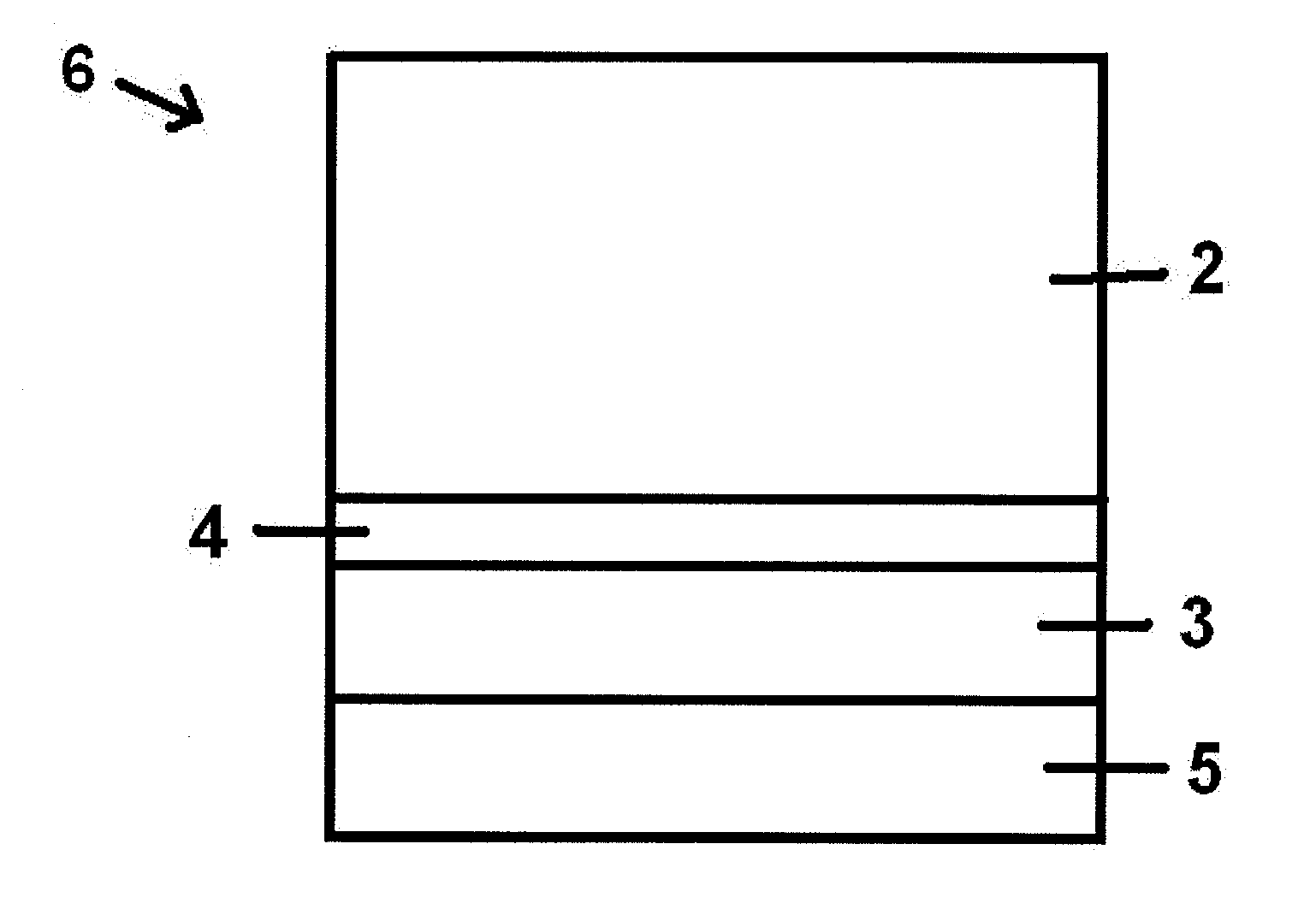
Electronic device and process for manufacturing the same
a technology of electronic devices and manufacturing processes, applied in the field of electronic devices, can solve problems such as the effect of increasing the drive current, affecting the electric properties of the dielectric material, and tunnelling current leakage problems
- Summary
- Abstract
- Description
- Claims
- Application Information
AI Technical Summary
Benefits of technology
Problems solved by technology
Method used
Image

Examples
example 1
[0059]A silicon wafer was coated with 2.5 nm of HfSiO by atomic layer CVD with an atomic ratio hafnium / silicon of 60 / 40. A HfSiON layer was then obtained by subjecting HfSiO to a plasma nitridation. A 1 nm layer of HfO2 was then deposited on top of the HfSiON layer. The assembly obtained was degassed for 4 minutes at 350° C. and a 10 nm layer of Ta2C was deposited on top of the assembly by means of physical vapour deposition. The resulting assembly was then capped with an additional Poly-Si layer and annealed at about 1030° C. for 1 second. The work-function of the device obtained was measured as 4.45 eV.
example 2
[0066]A silicon wafer was coated with 2.5 nm of a HfSiO layer by means of atomic layer CVD with an atomic ratio hafnium / silicon of 60 / 40. A HfSiON layer was then obtained by subjecting the HfSiO layer to a plasma nitridation. 1 nm of a HfO2 layer was then deposited on top of the HfSiON layer. The obtained assembly was degassed for 4 minutes at 350° C. and a 10 nm layer of TaC was deposited on top of it by means of physical vapour deposition. The resulting assembly was then capped with a Poly-Si layer and annealed at about 1050° C. under He atmosphere for 1.5 second.
example 3
[0067]A silicon wafer was coated with 2.5 nm of a HfSiO layer by means of atomic layer CVD with an atomic ratio hafnium / silicon of 60 / 40. A HfSiON layer was then obtained by subjecting the HfSiON layer to plasma nitridation. A 2 nm layer of HfO2 was then deposited on top of the HfSiON layer. The obtained assembly was degassed for 4 minutes at 350° C. and a 10 nm layer of TaC was deposited on top of it by means of physical vapour deposition. The resulting assembly was then capped with a Poly-Si layer and annealed at about 1050° C. under He atmosphere for 1.5 second.
PUM
 Abstract
Description
Claims
Application Information
 - R&D
- Intellectual Property
- Life Sciences
- Materials
- Tech Scout
- Unparalleled Data Quality
- Higher Quality Content
- 60% Fewer Hallucinations
Browse by: Latest US Patents, China's latest patents, Technical Efficacy Thesaurus, Application Domain, Technology Topic, Popular Technical Reports.
© 2025 PatSnap. All rights reserved.Legal|Privacy policy|Modern Slavery Act Transparency Statement|Sitemap|About US| Contact US: help@patsnap.com