Method of Reducing Detrimental STI-Induced Stress in MOSFET Channels

a technology of mosfet and sti, which is applied in the field of shallow trenchisolation-induced stress reduction of mosfet, can solve the problems of sti-induced stress being a component of undesirable narrow width effect, affecting the performance of drive current, and reducing mobility, so as to reduce stress, minimize thermal expansion, and reduce stress

Inactive Publication Date: 2008-07-17
VEECO INSTR
View PDF26 Cites 3 Cited by
  • Summary
  • Abstract
  • Description
  • Claims
  • Application Information

AI Technical Summary

Benefits of technology

[0009]In the present invention, a method of reducing stress induced by shallow trench isolation (STI) during MOSFET fabrication in a complementary metal-oxide semiconductor fabrication (CMOS) process is disclosed. In addition, this method also utilizes rapid thermal annealing (RTA) and laser annealing to form a shallower source / drain junction, which is necessary for advanced complementary metal-oxide semiconductors (CMOS) device scaling. The process according to the present invention is compatible with conventional CMOS fabrication techniques. A nitride cap is deposited before an n-well and / or p-well annealing to activate the dopants in the respective N and / or P wells. During the anneal, the nitride cap is expected to minimize the thermal expansion from STI, hence less stress is introduced into the silicon active regions. This state of lower stress will be retained or “memorized” by the STI and the surrounding Si device areas, as long as there is no subsequent high temperature anneal performed afterwards.

Problems solved by technology

A cause of performance degradation of the drive current is the mobility degradation due to local stress.
In addition, the stress induced by STI is a component of undesirable narrow width effect.
However, for example, oxide, nitride and silicon, have different thermal expansion coefficients, and thus it is difficult to control the stress or minimize the harmful stress.

Method used


Image

  • Method of Reducing Detrimental STI-Induced Stress in MOSFET Channels
  • Method of Reducing Detrimental STI-Induced Stress in MOSFET Channels
  • Method of Reducing Detrimental STI-Induced Stress in MOSFET Channels

Examples


first embodiment

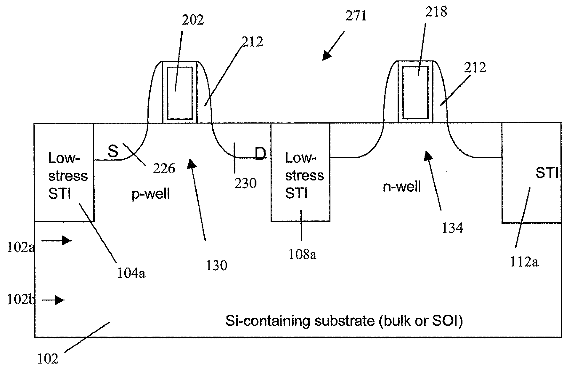
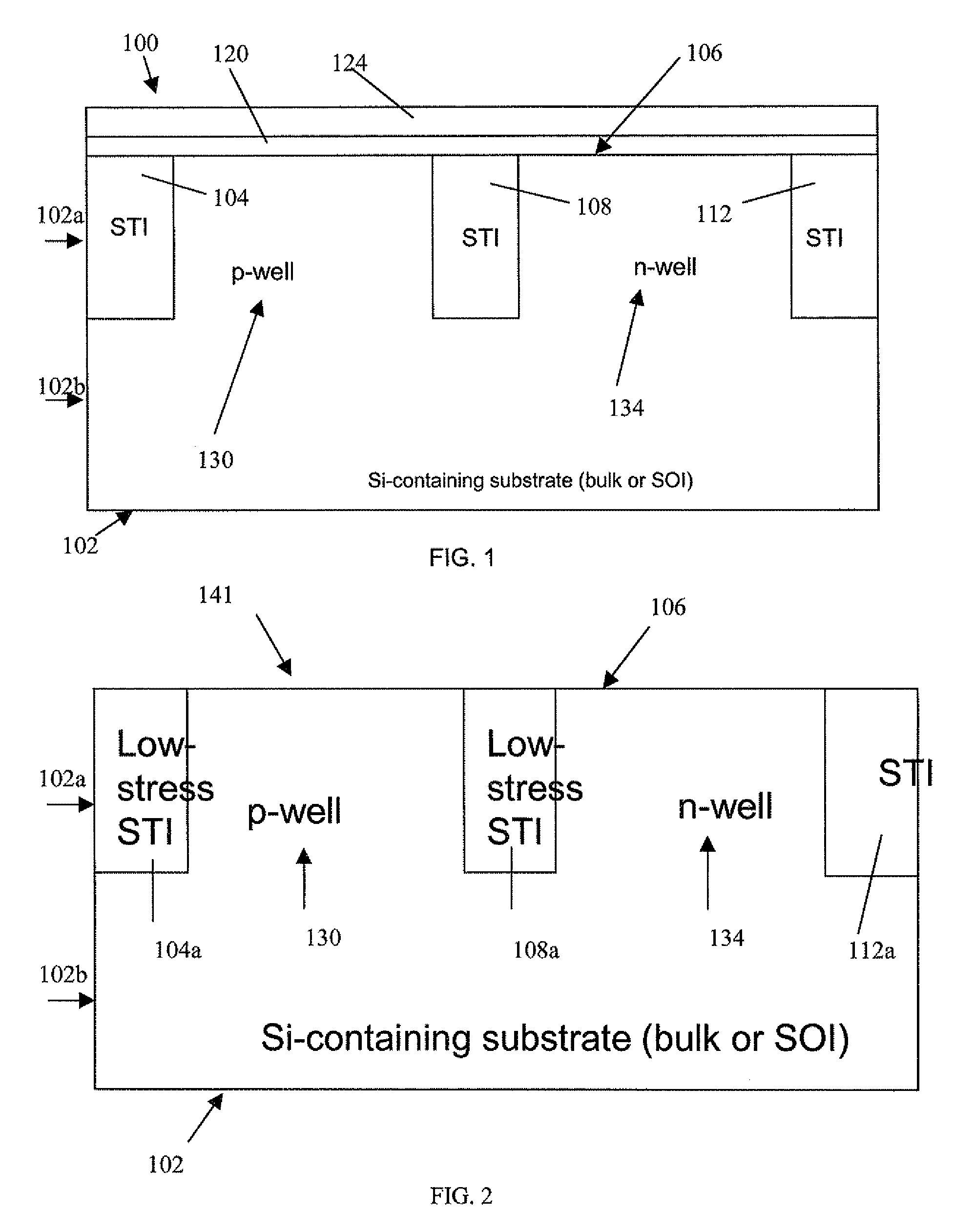
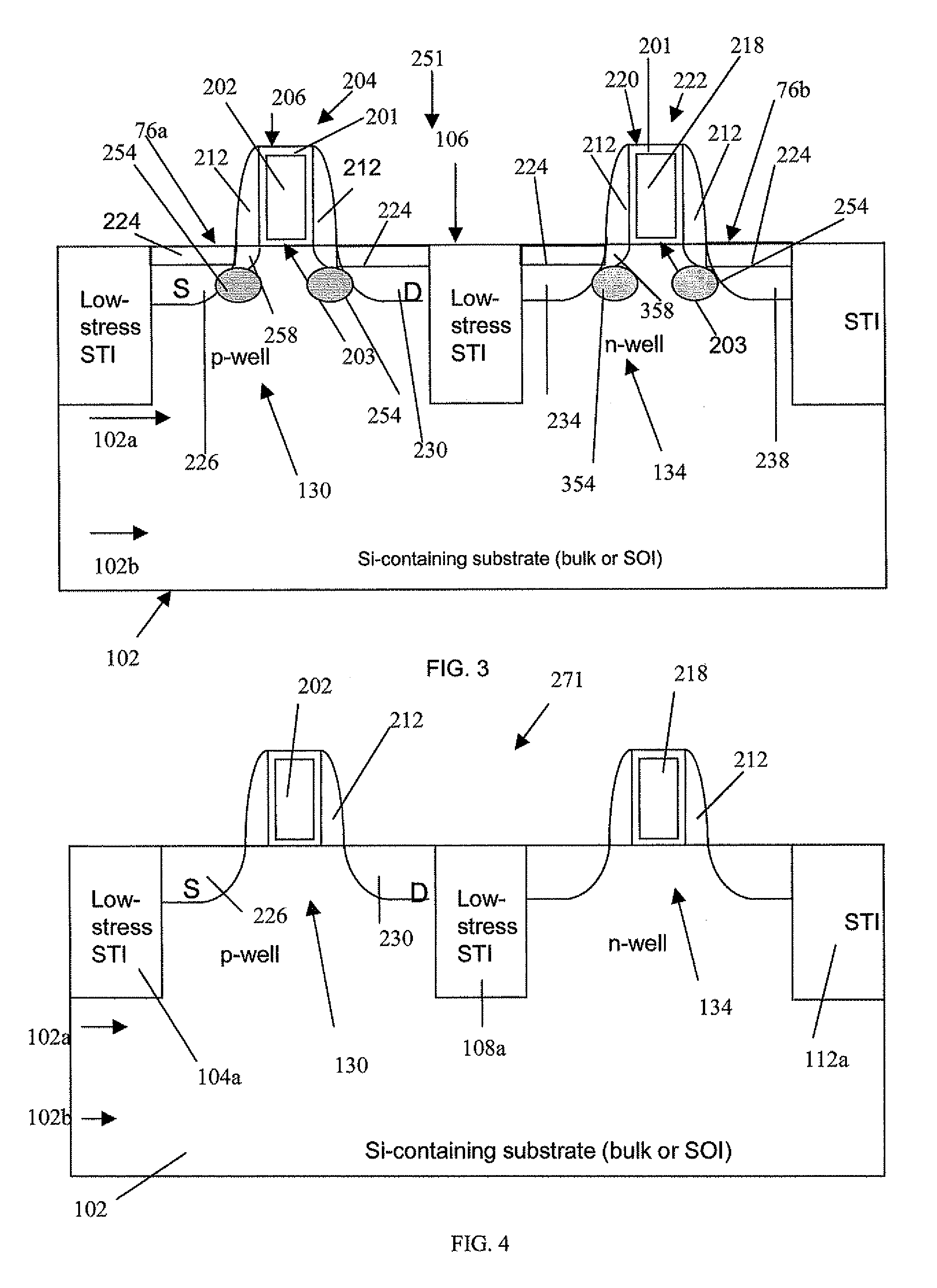
[0029]the method according to the present invention is depicted in FIGS. 1-3 for reducing detrimental STI-induced stress in MOSFET channels during their fabrication. Referring to FIG. 1, a substrate 102 can be, for example, a bulk wafer or SOI, or a substrate comprising silicon, such as SOI (silicon on insulator), bulk silicon, Silicon Germanium-on-insulator (SGOI), Strained silicon directly on insulator (SSDOI).

[0030]The top surface 106 of the substrate 102 is typically cleaned before the process begins to remove any residual layers (e.g., native oxide), foreign particles, and any residual metallic surface contamination and to temporarily protect the cleaned substrate surface. Any residual silicon oxide is first removed, for example, in a solution of hydrofluoric acid.

[0031]Referring to FIG. 1, first formed on the substrate 102 are shallow trench isolation (STI) regions 104, 108, 112, then p-well 130, and n-well 134 regions. The STI regions are typically formed of insulator materia...


PUM

PropertyMeasurementUnit
temperaturesaaaaaaaaaa
temperatureaaaaaaaaaa

Abstract

A method for reducing STI processing induced stress on a substrate during fabrication of a MOSFET. The method includes providing a substrate, wells (including dopants), and STIs in an upper layer of the substrate. A layer of an oxide substance is formed on a top surface of the upper layer of the substrate covering the STIs. A layer of a nitride substance is formed over the oxide layer. The substrate is annealed using temperatures greater than 1000° C. to activate the dopants in the wells which results in less stress on the STIs and hence less stress in the channels because of the nitride substance layer. The nitride and oxide substance layers are then stripped off the substrate, and CMOS fabrication is continued. The low stress remains in the channels if the thermal budget in following processes are low by using low temperature RTA and/or laser anneal.

Description

FIELD OF THE INVENTION[0001]This invention relates to a method for reducing shallow-trench-isolation-induced stress during fabricating complementary metal-oxide semiconductors (CMOS) devices, and more particularly, complementary metal-oxide-semiconductor field-effect transistors (MOSFETs).BACKGROUND OF THE INVENTION[0002]Complementary metal-oxide semiconductors (CMOS), are a major class of integrated circuits (IC). CMOS chips include microprocessors, microcontrollers, static RAM, and other digital logic circuits and RF / analog circuits.[0003]Generally CMOS processing includes forming multiple shallow trench isolation (STI) regions in a top layer of a substrate. The STI regions are typically formed so as to isolate, for example, a device region in a silicon on insulator (SOI) or bulk substrate, from another device region. A plurality of wells, e.g. p-wells, n-wells, can also be formed in the device region. For example, a p-well is formed of p-type semiconductor material, and an n-well...

Claims


Application Information

Patent Timeline
Patent Type & Authority Applications(United States)
IPC IPC(8): H01L21/26H01L21/8238
CPCH01L21/823807H01L21/823878H01L29/7846H01L29/665H01L29/1083
Inventor LEONG, MEIKEIOUYANG, QIQING C.SUNG, CHUN-YUNG
Owner VEECO INSTR
Why Eureka
Try Eureka