Semiconductor light-emitting device and method of manufacturing the same

a technology of semiconductors and light-emitting devices, which is applied in the direction of valve housings, mechanical devices, engine components, etc., can solve the problems of difficult to apply the above-described laminating structure using the junction metal layer, difficult to increase only adhesion, etc., to reduce the tendency to peel, increase the adhesion of the reflective metal layer, and increase the effect of only adhesion

Inactive Publication Date: 2008-07-24
SONY CORP
View PDF5 Cites 34 Cited by
  • Summary
  • Abstract
  • Description
  • Claims
  • Application Information

AI Technical Summary

Benefits of technology

[0007]To reduce the tendency to peel in the semiconductor light-emitting device with the ODR structure, it is necessary to increase the adhesion of the reflective metal layer to the insulating layer; however, it is difficult to increase only adhesion wit

Problems solved by technology

To reduce the tendency to peel in the semiconductor light-emitting device with the ODR structure, it is necessary to increase the adhesion of the reflective metal layer to the insulating layer; however, it is difficult to increase only adhesion with the related art structure in which the reflective metal layer is directly laminated on the insulating layer.
In general, the compound semiconductor layer is formed so as to have a very thin thickness, so when a substrate for growth is removed, subsequent handling is very difficult; however, in the manufacturing method, the device itself is reinforced by the bonded metal layer or supporting substrate, and the handling ability af

Method used


Image

  • Semiconductor light-emitting device and method of manufacturing the same
  • Semiconductor light-emitting device and method of manufacturing the same
  • Semiconductor light-emitting device and method of manufacturing the same

Examples


examples

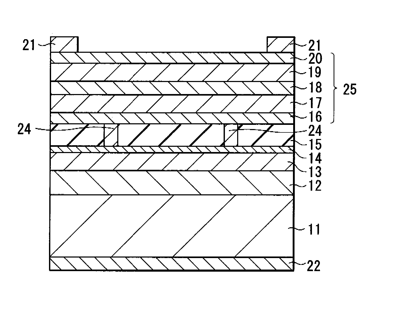
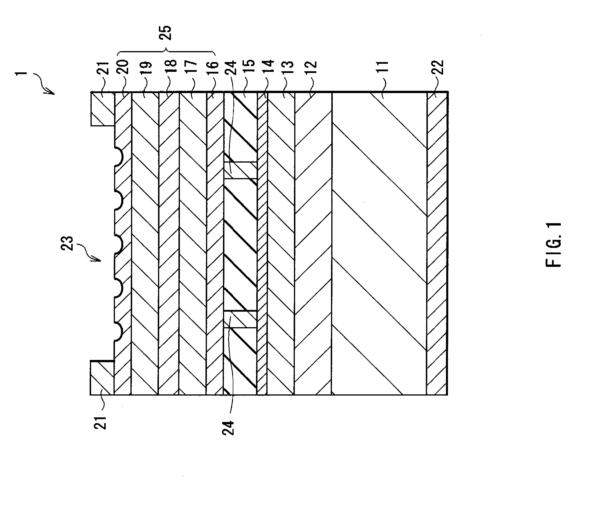
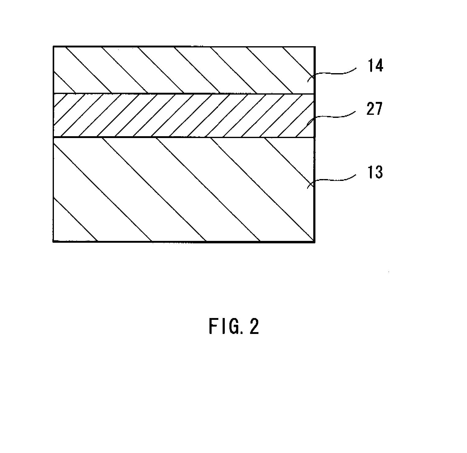
[0044]Here, changes in reflectivity by providing the first metal layer 14 between the insulating layer 15 and the reflective layer (the second metal layer 13) were studied, compared to the case of using only the reflective layer. More specifically, as the insulating layer, a glass substrate was used, and a metal layer made of Al and a metal layer made of Au were deposited on the glass substrate in order, and light entered from the glass substrate side to measure reflectivity. FIGS. 5 and 6 show a relationship between light-emitting wavelengths and reflectivity at that time.

[0045]At first, a plot of FIG. 5 shows measurement results in the case where an Al layer was not laminated (indicated by D in the plot) and the cases where the thickness of the Al layer was 10 nm, and the thickness of the Au layer was 200 nm (indicated by A in the plot), 300 nm (indicated by B in the plot) and 400 nm (indicated by C in the plot). An annealing process after laminating Al was performed at 400° C. In...


PUM


Abstract

A semiconductor light-emitting device includes: a semiconductor layer including a light-emitting region and having an emission surface on its surface; an insulating layer arranged on a surface of the semiconductor layer opposite to; a first metal layer deposited on a surface of the insulating layer opposite to a surface where the semiconductor layer is arranged; a contact portion buried in a part of the insulating layer, the contact portion electrically connecting the semiconductor layer and the first metal layer; and a second metal layer having higher reflectivity with respect to a light-emitting wavelength than the first metal layer, the second metal layer arranged on a surface of the first metal layer opposite to a surface where the insulating layer is arranged, wherein a metal of which the first metal layer is made has higher adhesion to the insulating layer than a metal of which the second layer is made.

Description

[0001]The present invention contains subject matter related to Japanese Patent Application JP 2006-042071 filed in the Japanese Patent Office on Feb. 20, 2006, the entire contents of which being incorporated herein by reference.BACKGROUND OF THE INVENTION[0002]1. Field of the Invention[0003]The present invention relates to a semiconductor light-emitting device having an ODR (Omni-Directional-Reflector) structure and a method of manufacturing the same.[0004]2. Description of the Related Art[0005]In recent years, there is a demand for semiconductor light-emitting devices such as high-power light-emitting diodes as light sources for liquid crystal displays and projectors. One of them is a light-emitting diode having an ODR structure for extracting emitted light in one direction (refer to Japanese Unexamined Patent Application Publication No. S52-37783). In the ODR structure, an insulating layer made of SiO2 (silicon dioxide) or the like is arranged between a semiconductor layer having ...

Claims


Application Information

Patent Timeline
IPC IPC(8): H01L33/00H01L21/00H01L33/38H01L33/40
CPCH01L33/405H01L33/0079H01L33/0093F16K3/0209F16K51/00F16K27/04
Inventor KUROMIZU, YUICHI
Owner SONY CORP
Why Eureka
Try Eureka