Gallium nitride on silicon with a thermal expansion transition buffer layer

Inactive Publication Date: 2008-07-24
SHARP LAB OF AMERICA
View PDF39 Cites 25 Cited by
  • Summary
  • Abstract
  • Description
  • Claims
  • Application Information

AI Technical Summary

Benefits of technology

[0014]The present invention provides a means for matching the TEC of a Si substrate with that of a GaN film deposited on the Si substrate. The TEC of the Si substrate is modified by depositing a layer structure on Si, which has a TEC that more closely matches the TEC of the GaN film.

Problems solved by technology

However, these substrates are expensive to make, and their small size also drives fabrication costs.
The low thermal and electrical conductivity constraints associated with sapphire make device fabrication more difficult.
This contact configuration complicates contact and package schemes, resulting in a spreading-resistance penalty and increased operating voltages.
The poor thermal conductivity of sapphire, as compared with that of Si or SiC, also prevents efficient dissipation of heat generated by high-current devices, such as laser diodes and high-power transistors, consequently inhibiting device performance.
There are two fundamental problems associated with GaN-on-Si device technology.
First, there is a lattice mismatch between Si

Method used


Image

  • Gallium nitride on silicon with a thermal expansion transition buffer layer
  • Gallium nitride on silicon with a thermal expansion transition buffer layer
  • Gallium nitride on silicon with a thermal expansion transition buffer layer

Examples


Embodiment Construction

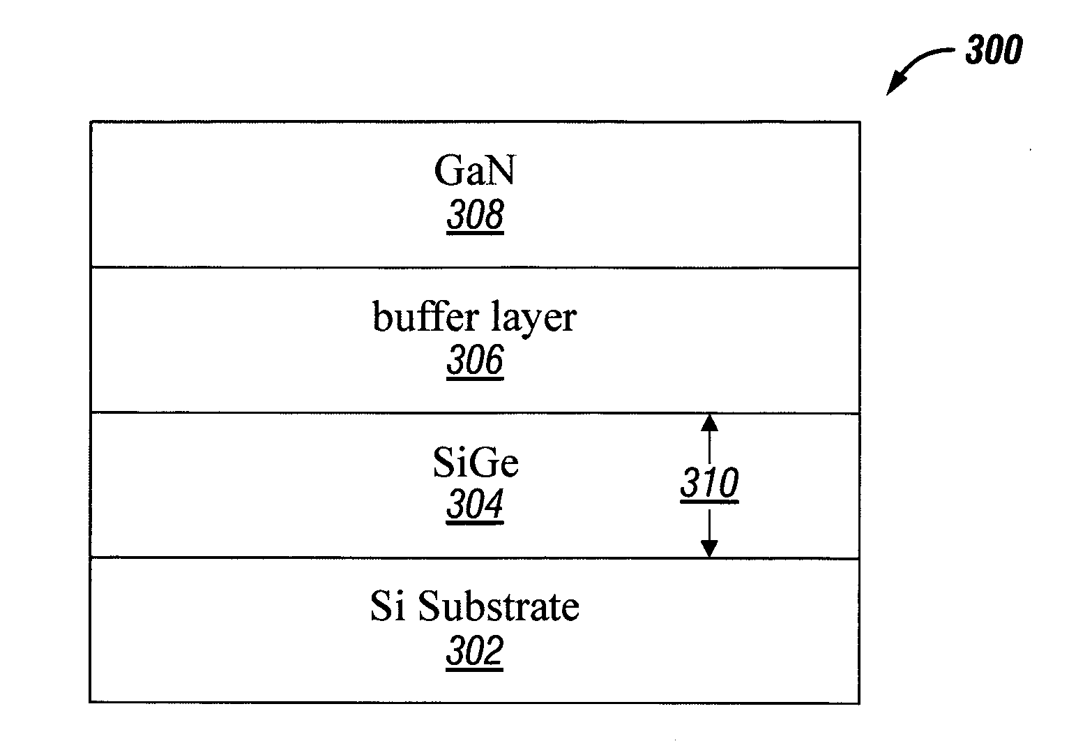
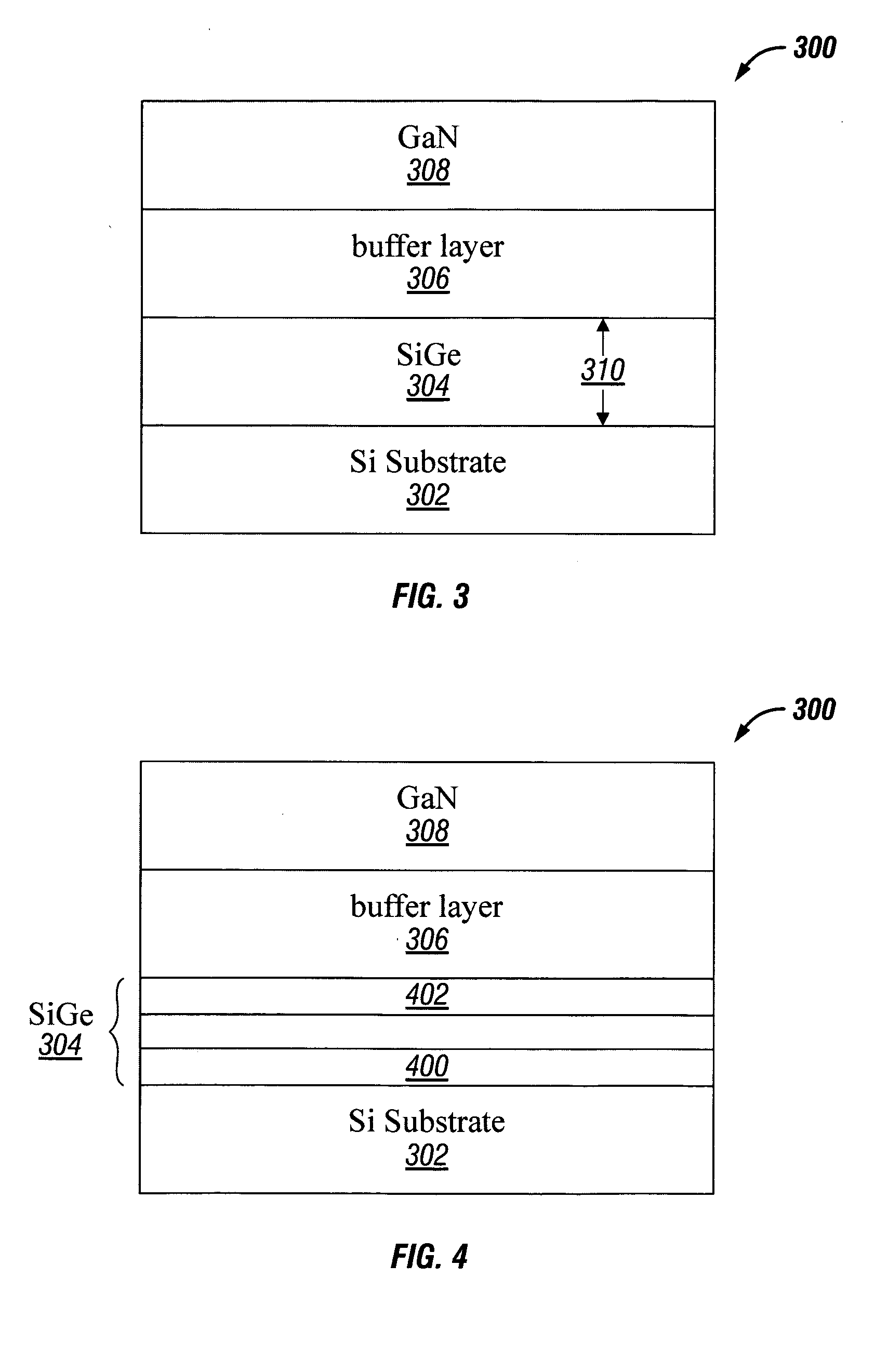
[0029]FIG. 3 is a partial cross-sectional view of a gallium nitride (GaN)-on-silicon (Si) structure with a thermal expansion interface. The structure 300 comprises a (111) Si substrate 302 with a first thermal expansion coefficient (TEC). A silicon-germanium (SiGe) film 304 overlies the Si substrate 302. A buffer layer 306 overlies the SiGe film 304. For example, the buffer layer 306 may be either aluminum nitride (AlN) or aluminum-gallium nitride (AlGaN). However, other buffer layer materials are known in the art, that although less desirable in some circumstances, may also be used. A GaN film 308 overlies the buffer layer 306, having a second TEC. The SiGe film 304 has a third TEC, with a value in between the first and second TECs.

[0030]Generally, the SiGe film 304 may have a thickness 310 in the range of about 200 nanometers (nm) to 4 micrometers. In one aspect, the SiGe film 304 has a non-varying Ge content in a range of about 10 to 50%, and a thickness 310 in a range of about 1...


PUM


Abstract

A method is provided for forming a matching thermal expansion interface between silicon (Si) and gallium nitride (GaN) films. The method provides a (111) Si substrate with a first thermal expansion coefficient (TEC), and forms a silicon-germanium (SiGe) film overlying the Si substrate. A buffer layer is deposited overlying the SiGe film. The buffer layer may be aluminum nitride (AlN) or aluminum-gallium nitride (AlGaN). A GaN film is deposited overlying the buffer layer having a second TEC, greater than the first TEC. The SiGe film has a third TEC, with a value in between the first and second TECs. In one aspect, a graded SiGe film may be formed having a Ge content ratio in a range of about 0% to 50%, where the Ge content increases with the graded SiGe film thickness.

Description

BACKGROUND OF THE INVENTION[0001]1. Field of the Invention[0002]This invention generally relates to integrated circuit (IC) fabrication and, more particularly, to a gallium nitride / silicon (Si) thermal expansion interface and associated fabrication process.[0003]2. Description of the Related Art[0004]Gallium nitride (GaN) is a Group III / Group V compound semiconductor material with wide bandgap (3.4 eV), which has optoelectronic, as well as other applications. Like other Group III nitrides, GaN has a low sensitivity to ionizing radiation, and so, is useful in solar cells. GaN is also useful in the fabrication of blue light-emitting diodes (LEDs) and lasers. Unlike previous indirect bandgap devices (e.g., silicon carbide), GaN LEDs are bright enough for daylight applications. GaN devices also have application in high power and high frequency devices, such as power amplifiers.[0005]GaN LEDs are conventionally fabricated using a metalorganic chemical vapor deposition (MOCVD) for deposit...

Claims


Application Information

Patent Timeline
IPC IPC(8): H01L29/267H01L21/20
CPCH01L21/02381H01L21/02433H01L21/0245H01L21/02458H01L21/02502H01L29/267H01L21/0254H01L21/02656H01L29/045H01L29/2003H01L21/0251
Inventor MAA, JER-SHENLI, TINGKAITWEET, DOUGLAS J.STECKER, GREGORY M.HSU, SHENG TENG
Owner SHARP LAB OF AMERICA
Why Eureka
Try Eureka