Mobile Charge Induced Periodic Poling and Device

a mobile charge and periodic poling technology, applied in non-linear optics, electric/magnetic/electromagnetic heating, instruments, etc., can solve the problems of domain limit lateral dimensions and efficiency, difficult to grow long lengths, and inversion of domains

Active Publication Date: 2008-07-24
NECSEL INTPROP
View PDF4 Cites 13 Cited by
  • Summary
  • Abstract
  • Description
  • Claims
  • Application Information

AI Technical Summary

Benefits of technology

[0017]Accordingly, an object of the present invention is to provide a domain grating device, and its associated fabrication methods, that has controlled domain growth through the bulk of a crystal substrate for uniform short period domain inversion gratings.

Problems solved by technology

This method can produce gratings with periods as short as 6 μm and 4 μm, but it is difficult to grow long lengths and curvature of the domains limits the lateral dimensions and efficiency.
Impurity doping or material removal in some ferroelectric materials (such as lithium niobate and KTP) can result in domain inversion.
Short period domain inversion in Z-cut congruent lithium niobate (CLN) was first demonstrated by Yamada at Sony in 1992 (U.S. Pat. No. 5,193,023) but the described process suffered from limitations in the material thickness and high instances of destructive electrical breakdown.
These localized trapped electrons in the material result in localized high electric field that causes domain inversion.
However the MgO dopant in MgO:CLN brings an even bigger challenge in realizing periodic domain structures.
However, short-period-domain-grating structures have not been achieved at room temperature in a reliable and repeatable manner.
This current flow results in preferential growth of domains which are formed early in the poling process and disrupts the domain seeding uniformity and therefore the uniformity of the final grating pattern.
Since the inverted domain structure does not strictly follow the crystal structure, it is fundamentally challenging for the inverted domain to propagate through the entire thickness of the substrate while maintaining the lateral dimensions of the masking pattern applied on one surface of the substrate.

Method used


Image

  • Mobile Charge Induced Periodic Poling and Device
  • Mobile Charge Induced Periodic Poling and Device
  • Mobile Charge Induced Periodic Poling and Device

Examples


Embodiment Construction

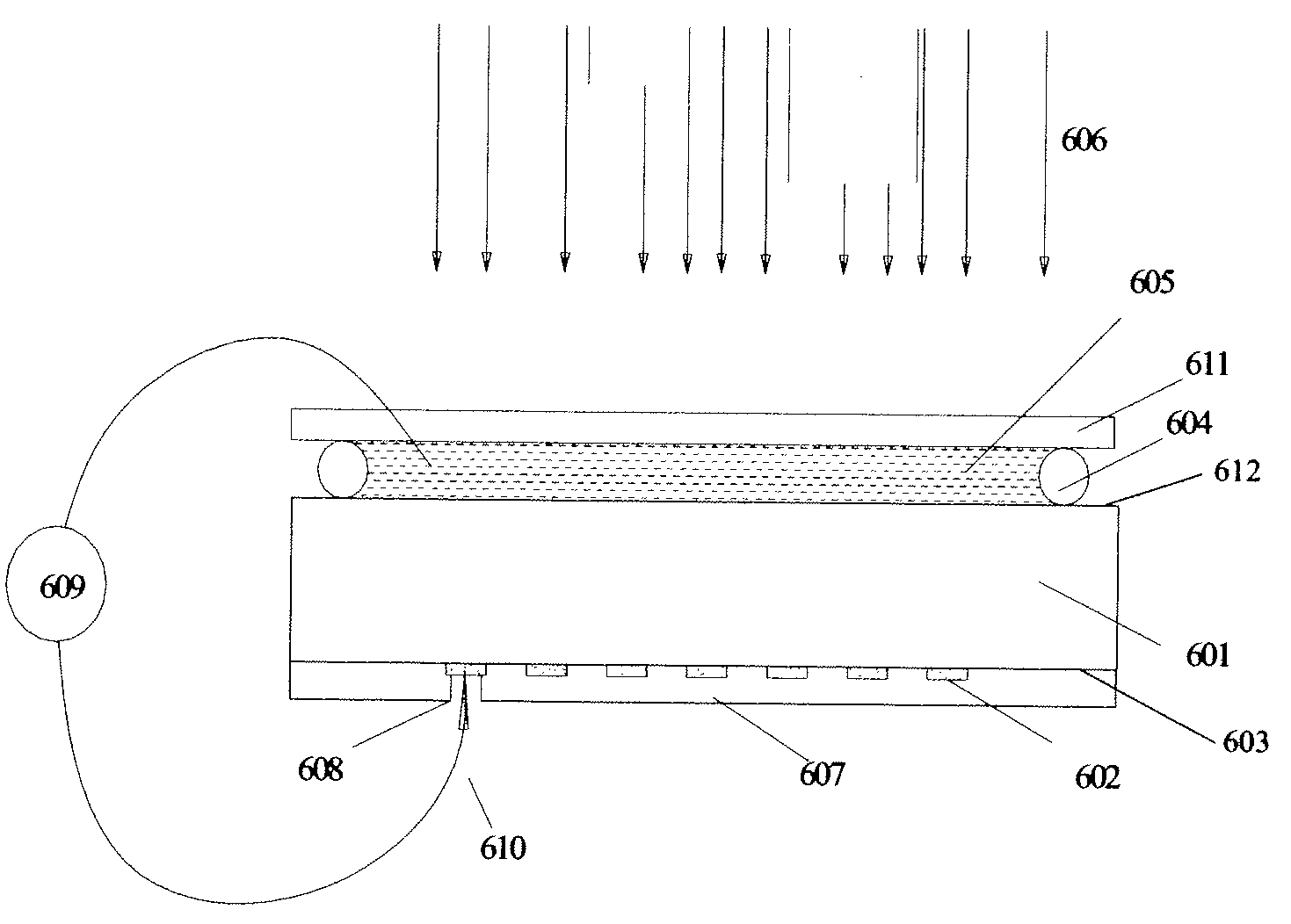
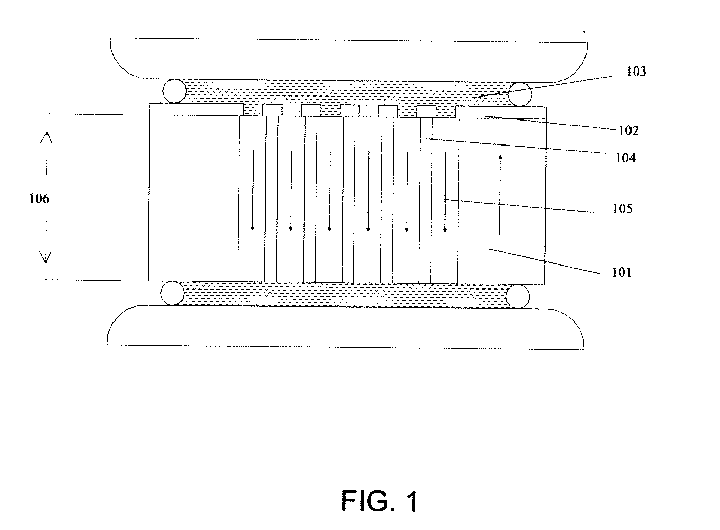
[0042]In one embodiment of the present invention, an improved domain inversion structure is provided that has optimized efficiency, reliable fabrication and ease of characterization. This improved domain inversion structure is the result of a new high voltage electric field poling based fabrication process which involves the generation of mobile charges within the substrate that is to be poled, accompanied by the application of a patterned high voltage electric field. This combination results in a patterned current flow through the substrate and creates a patterned domain inversion structure within the substrate. Various combinations of charge generation and voltage application can be used to tailor the size and shape of the domain inverted regions.

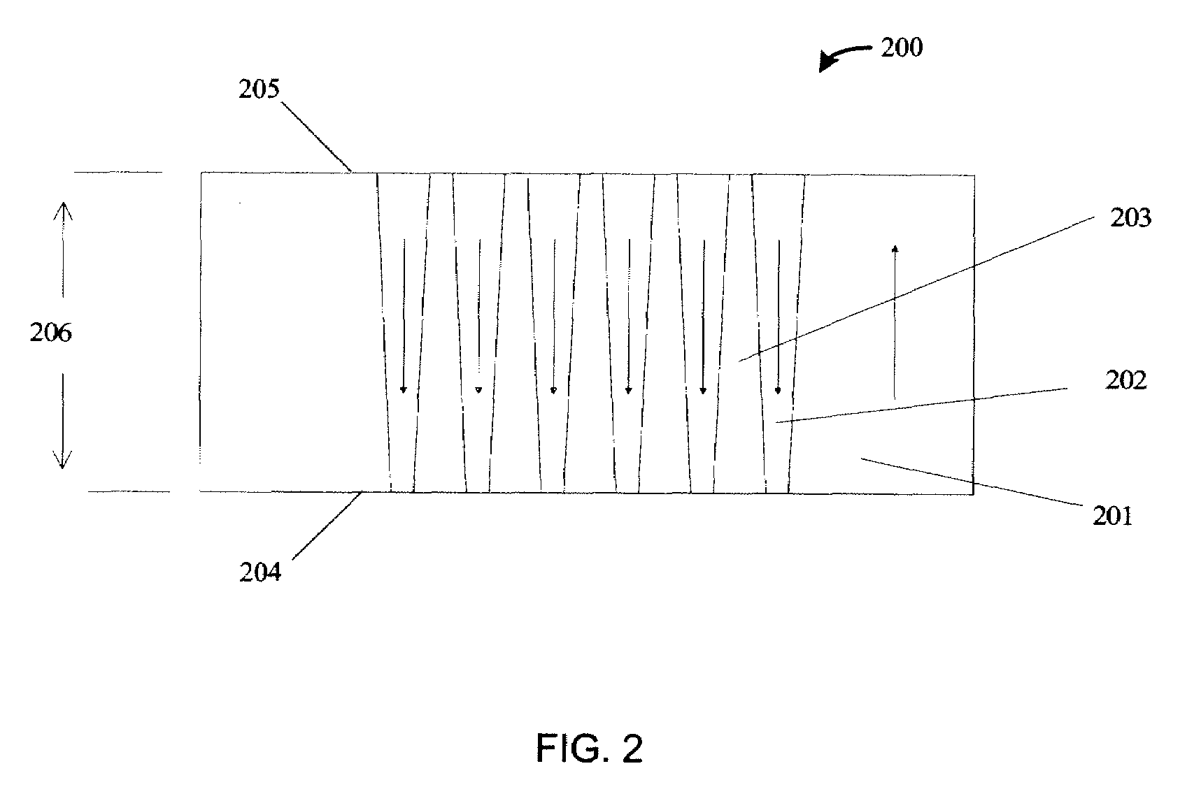
[0043]In one embodiment, as illustrated in FIG. 2, a frequency conversion device 200 is provided. An improved domain inversion structure resulting from a new fabrication process is shown schematically in FIG. 2. The inverted domains 202 a...


PUM


Abstract

Devices and methods are disclosed for realizing a high quality bulk domain grating structure utilizing mobile charges that are generated by means of photo-excitation in a substrate. An effect of light exposure (UV, visible, or a combination of wavelengths) is to generate photo-induced charges. The application of a voltage across the substrate combined with the application of light exposure causes a photo-induced current to flow through the substrate. The photo-induced charges (behaving like virtual electrode inside the material) and the photo-induced current result in both reduction of the coercive field required for domain inversion in the material and improve realization of the domain inversion pattern, which previously has not been possible at room temperature.

Description

CROSS-REFERENCE TO RELATED APPLICATIONS[0001]This application is a continuation-in-part of U.S. Ser. No. 11 / 530,336, filed Sep. 8, 2006, which application is fully incorporated herein by reference.BACKGROUND OF THE INVENTION[0002]1. Field of the Invention[0003]This invention relates generally to high quality short period bulk domain inversion structures (gratings), and more particularly to high quality short period bulk domain inversion structures (gratings) that are fabricated in substrate materials such as MgO doped congruent lithium niobate using electric field poling.[0004]2. Description of the Related Art[0005]Quasi phase matching (QPM) is an efficient way to achieve nonlinear optical interactions. The approach was first proposed by Bloembergen et al. (U.S. Pat. No. 3,384,433), using a domain inversion grating structure to achieve QPM. Such a domain grating structure can be usefully realized in an optically transparent ferroelectric material, such as lithium niobate (LiNbO3), l...

Claims


Application Information

Patent Timeline
Patent Type & Authority Applications(United States)
IPC IPC(8): G03B21/14H05B6/00H01S3/109
CPCG02F1/3544G03B21/14G02F1/3775G02F1/3558
Inventor HUANG, LEE LISHENGFIELD, SIMON JOHN
Owner NECSEL INTPROP
Why Eureka
Try Eureka