Semiconductor memory device and test method thereof

a memory device and semiconductor technology, applied in semiconductor/solid-state device testing/measurement, solid-state devices, instruments, etc., can solve the problems of difficult to reduce the chip size and fabricate a package, difficult to fabricate a package including 500 ball-outs or more, and difficult to perform pad probing

Active Publication Date: 2008-07-24
SAMSUNG ELECTRONICS CO LTD
View PDF9 Cites 26 Cited by
  • Summary
  • Abstract
  • Description
  • Claims
  • Application Information

AI Technical Summary

Benefits of technology

[0027]An embodiment of the invention provides a semiconductor memory device having a pad arrangement for fabricating a probe car

Problems solved by technology

Therefore, expansion of the input/output data bits makes it difficult to reduce a chip size and fabricate a package.
However, since the currently used BGA package has 225-460 pins, it is almost impossible to fabricate a package including 500 ball-outs or more.
In particular, since it is unmarketable to employ the BGA package to a semiconductor memory device for a mobile electronic appliance requiring a small package, new package manufacturing technologies, for example, p-bump (micro bump) technology, and so on, have been developed.
However, when the wafer of the semiconductor memory device fabricated as described above is tested, it can be impossible to perform the pad probing.
Specifically, a needle of a probe has a thickness of about 15 μm, and an error of about 5 μm or more is generated during positioning of the probe.
When the probe needle inappropriately contacts the pad, a contact error is generated, thereby making it difficult to properly perform the test.
As a result, when the pad has a width or length of 35 μm or less, it is difficult to obtain a secure contact, and when the pad pitch, i.e., an interval between pads, is smaller than 50 μm, the probe needle could be in bad contact with adjacent pads.
However, since a pad region is limited, the center pad structure is widely used to obtain a layout well matched with the memory cell array.
When the pads are disposed in a multi-row manner as shown in FIG. 1, since it is limiting to bond each pad to a lead end using a wire, the probe should be

Method used


Image

  • Semiconductor memory device and test method thereof
  • Semiconductor memory device and test method thereof
  • Semiconductor memory device and test method thereof

Examples


first embodiment

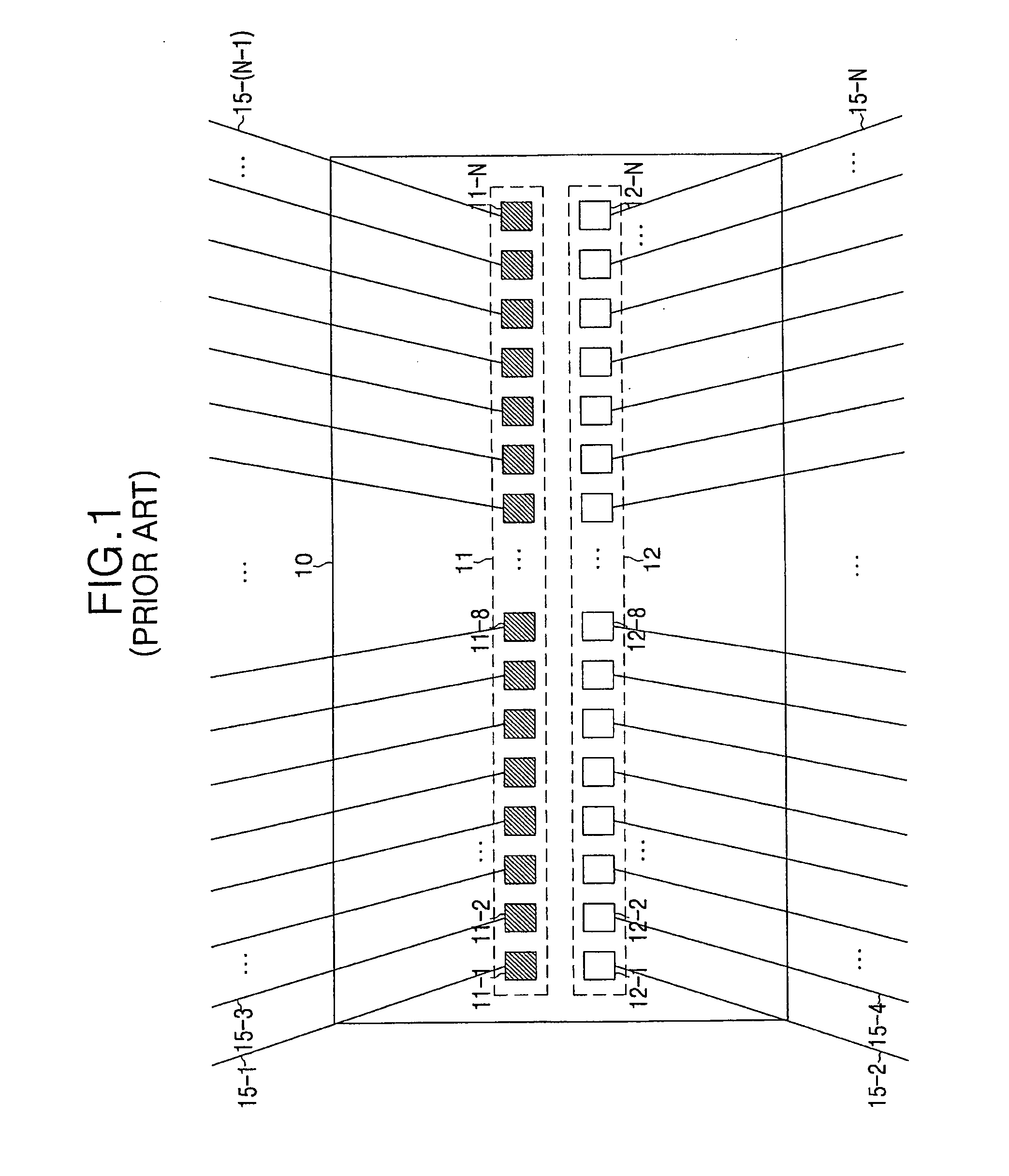
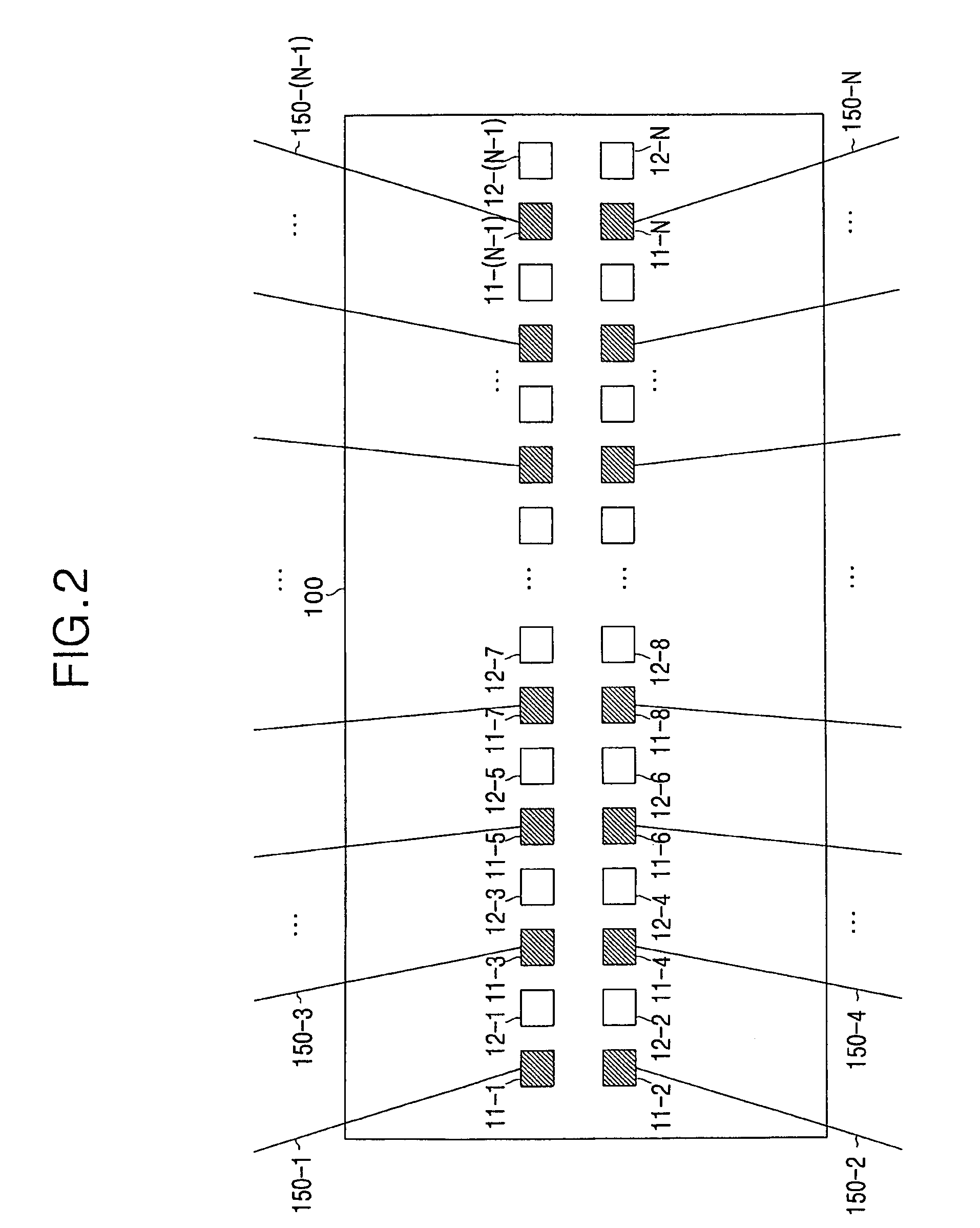
[0078]It is possible to solve this problem by enlarging only the pad pitch of the center pad structure shown in FIG. 2, because the plurality of probes 150-1 to 150-N of the probe card can incorrectly contact the plurality of first and second channel pads 20-1 to 20-N and 30-1 to 30-N due to a limitation of the pad size in the wafer test apparatus of the

[0079]That is, in order to overcome the problem, a plurality of pads are disposed to correspond to one channel in two rows to increase a pad size to fabricate the probe card having a large interval between the probes 150-1 to 150-N, thereby stably performing the test. Then, the test can be stably performed through the other of the first channel pads and the second channel pads using the probe card having the probes 150-1 to 150-N having the same interval.

[0080]In addition, in contrast to the test method of the first embodiment for testing a wafer having a large pad pitch shown in FIG. 2, when the wafer test is completed through one o...

third embodiment

[0101]The test method of the third embodiment is a method of grouping some pads having the same function as the plurality of channels to operate all of the channels using a small number of pads during a wafer test operation of the semiconductor memory device.

[0102]For example, when a plurality of data input / output signal pads, a plurality of address signal pads, and some command signal pads are all connected to the plurality of channels in the semiconductor memory device during a test mode operation, and some control signal pads, such as a chip selection signal (CS), are used for the plurality of channels, respectively, it is possible to test all of the channels using the small number of pads.

[0103]In FIGS. 4 and 5, the mode register 310 receives a set of external mode setting signals MA[12:0] through the plurality of address pads A1 to AN used to determine the normal mode, the first channel internal circuit test mode, or the second channel internal circuit test mode using lower thr...

second embodiment

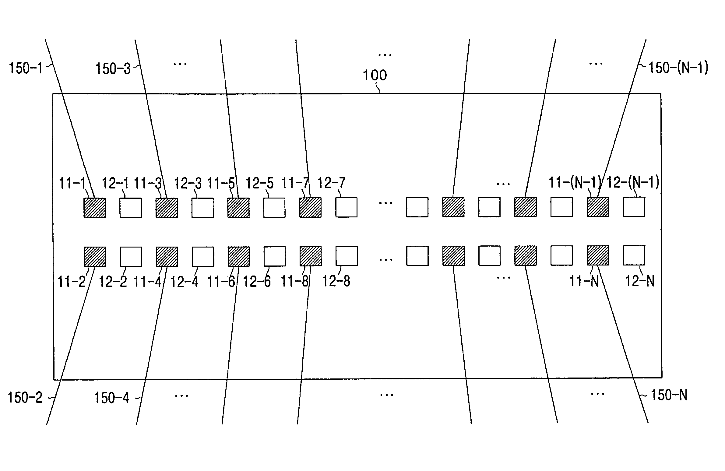
[0113]Therefore, in this embodiment, it is possible to solve the problem in which the plurality of probes 150-1 to 150-N of the probe card hardly contact the plurality of first and second channel pads 11-1 to 11-N and 12-1 to 12-N due to limitations of the pad size in the first pad pitch only in the center pad structure shown in FIG. 2, and to solve the problem in which the chip size is increased due to the increase in the number of pads in the second embodiment for testing a wafer by enlarging a pad pitch and a pad size of the center pad structure shown in FIG. 3.

[0114]As can be seen from the foregoing, a semiconductor memory device and a test method thereof in accordance with the present invention are capable of obtaining a secure contact with respect to pads by enlarging a pad pitch and a pad size during a wafer test of a semiconductor memory device, and performing all tests through a plurality of channel pads using a plurality of probes of a probe card without incorrect contact ...


PUM


Abstract

Provided are a semiconductor memory device and a test method thereof. The semiconductor memory device includes: a die in which a plurality of internal circuits are integrated; a plurality of first and second channel pads having a first pad size and a first pad pitch, disposed in an alternating manner in a straight line at a center part of the die, and divided into a plurality of parallel rows, wherein the plurality of first and second channel pads are configured to selectively contact test probes in an alternating manner to receive an external wafer test signal and to output a signal generated by the plurality of internal circuits to the exterior. Therefore, it is possible to perform a test using plural channel pads during a wafer test of the semiconductor memory device using a plurality of probes of a probe card without incorrect contacts or non-contact with adjacent pads.

Description

CROSS-REFERENCE TO RELATED APPLICATION[0001]This application claims priority under 35 U.S.C. §119 to Korean Patent Application No. 10-2007-0002958, filed Jan. 10, 2007, the disclosure of which is hereby incorporated herein by reference in its entirety.BACKGROUND OF THE INVENTION[0002]1. Field of the Invention[0003]The present invention relates to a semiconductor device memory, and more particularly, to a semiconductor memory device and a test method thereof capable of more stably and effectively performing a wafer test of the semiconductor memory device having a small pad size and a small interval between pads.[0004]2. Description of the Related Art[0005]Generally, a test process of a semiconductor memory device can be classified into a wafer test performed before a wafer is assembled and a package test performed in a package state after assembly. The wafer test can be classified into a pre-laser test performed before a laser repair process and an electronic die sorting (EDS) test p...

Claims


Application Information

Patent Timeline
IPC IPC(8): G11C29/00G11C7/00
CPCG01R31/318511G11C29/006G11C29/1201H01L2224/06156G11C29/56G11C2029/5602G11C29/48H01L22/00
Inventor KIM, YONG-JUNJEONG, WOO-SEOPLEE, KYU-CHAN
Owner SAMSUNG ELECTRONICS CO LTD
Why Eureka
Try Eureka