Two-dimensional arrays of holes with sub-lithographic diameters formed by block copolymer self-assembly

a self-assembly and block copolymer technology, applied in the direction of ohmic resistance heating, library creation, transportation and packaging, etc., can solve the problems of not being able to address the ordering of domains over a large area, not being able to control the location and orientation of ordered domains, and not being able to accommodate the fabrication of structures and features at the nanometer level

Active Publication Date: 2008-07-24
MICRON TECH INC
View PDF99 Cites 138 Cited by
  • Summary
  • Abstract
  • Description
  • Claims
  • Application Information

AI Technical Summary

Problems solved by technology

Optical lithographic processing methods are not able to accommodate fabrication of structures and features at the nanometer level.
However, that layout is not useful for making structures such as DRAM capacitors, which require a rectangular or square shaped array layout.
Although one-dimensional arrays have been formed in trenches, no efforts have been made to address ordering of the domains over a large area, or to control the location and orientation of ordered domains in two dimensions.

Method used


Image

  • Two-dimensional arrays of holes with sub-lithographic diameters formed by block copolymer self-assembly
  • Two-dimensional arrays of holes with sub-lithographic diameters formed by block copolymer self-assembly
  • Two-dimensional arrays of holes with sub-lithographic diameters formed by block copolymer self-assembly

Examples


example 1

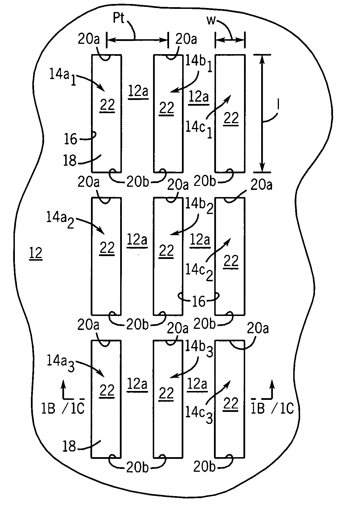
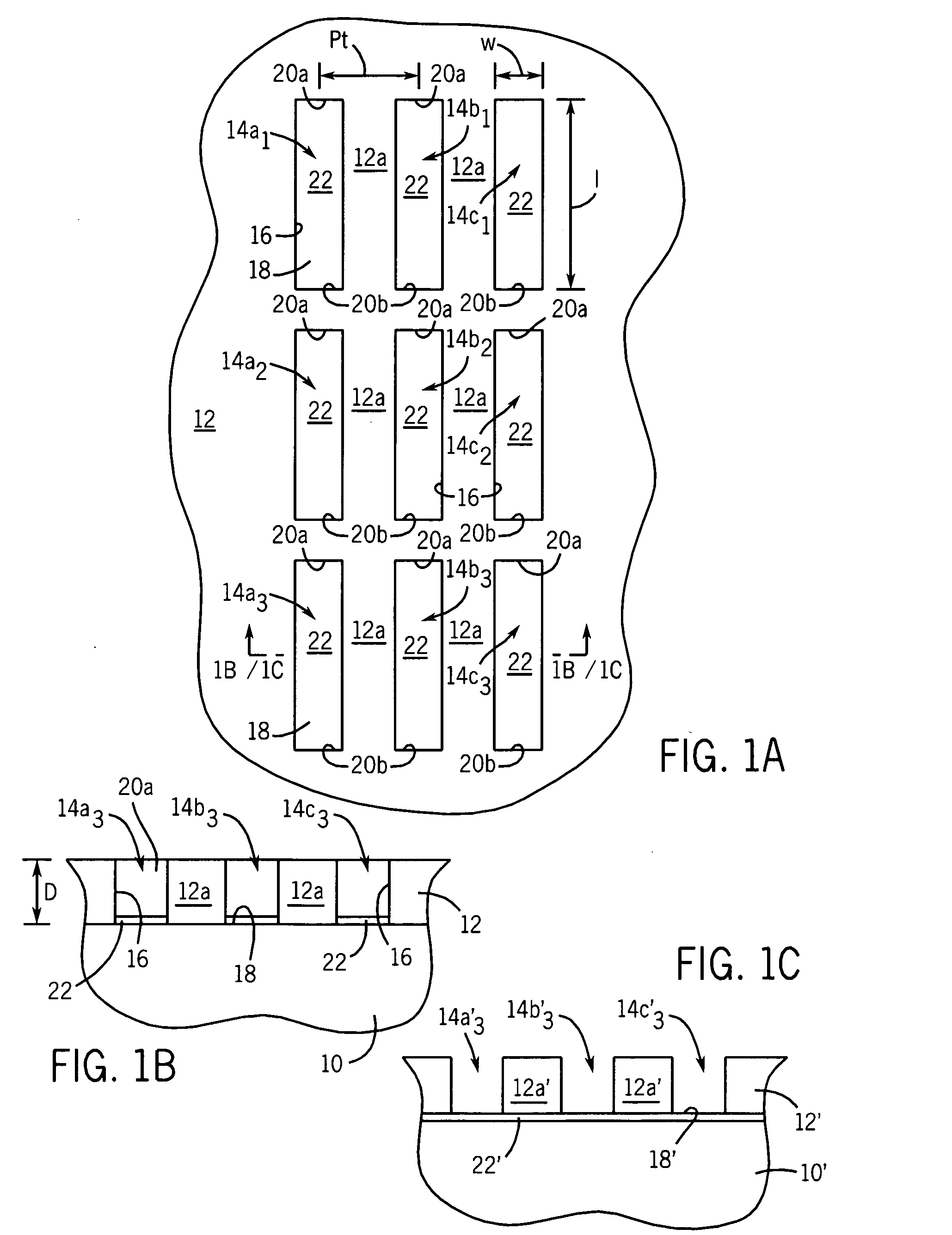
[0071]Trenches 250 nm deep with widths ranging from 75 nm to 600 nm having silicon oxide sidewalls and silicon oxycarbide floors were provided. On several of the wafers, oxide was deposited onto the sidewalls and the trench floors. Both types of trench floors were treated to be neutral wetting to PS and PMMA.

[0072]To get perpendicular cylinders, a random PS:PMMA copolymer solution (about 58% PS) containing a crosslinking agent was cast as a film of about 5-10 nm thick onto the features, and annealed at about 160° C. for 4 hours. Capillary forces pulled the PS-r-PMMA to the trench floor prior to complete cross-linking, leaving oxide sidewalls that were preferential-wetting to PMMA. The resulting trench structure had sidewalls that were preferential wetting with the random copolymer layer as a mat on the bottom of the trenches, which provided a neutral wetting surface.

[0073]A 0.425% solution of cylinder-forming PS-b-PMMA in toluene was then cast onto the treated substrates so as to fo...

example 2

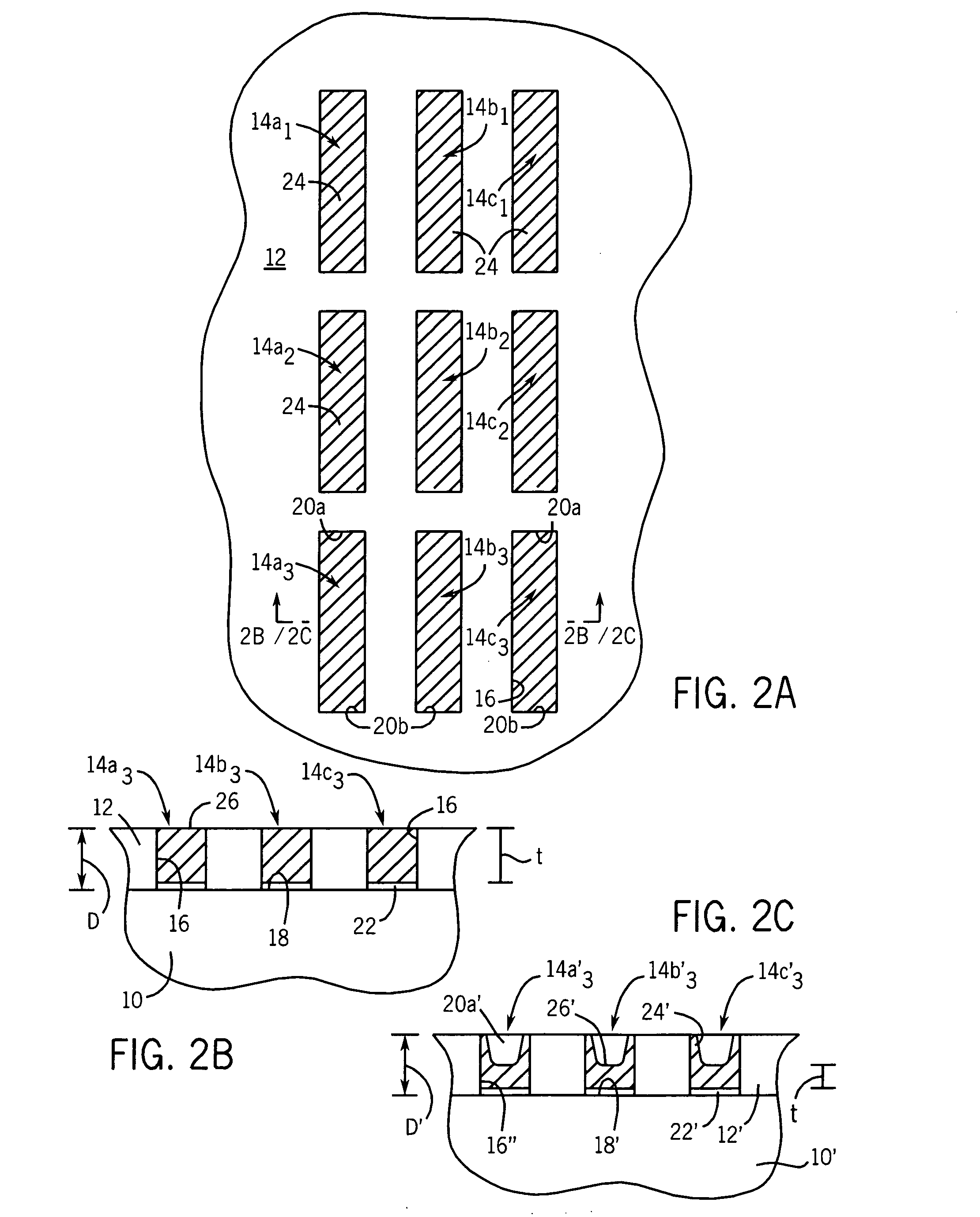
[0075]Ternary blends (10-40%) of homopolymers (20 K PS, 20 K PMMA) were prepared in 0.425% solutions of 46K / 21K PS-b-PMMA in toluene. These solutions were cast onto the substrates described above at thicknesses of 30-40 nm. The addition of homopolymers swells the domain sizes of the two fractions, resulting in an increased inherent pitch value (Lo) of the polymer.

[0076]At 10-20% homopolymers, a two row zigzag pattern of cylinders was formed as seen by SEM. With 30% homopolymers content, the zigzag pattern began to break down and numerous errors and unusual morphologies were observed. When a ternary blend of 46 / 21 PS-b-PMMA block copolymer with 40% 20 PS and 20K PMMA homopolymers was cast and annealed onto the same substrate (i.e., 80 nm wide trenches, (P(S-r-BCB-r-MMA)) floor, oxide sidewalls), single rows of perpendicular cylinders with apparent diameter of about 35 nm formed in the 80 nm wide trenches. At 40% homopolymers, the mixture caused a pitch of about 50 nm, resulting in th...


PUM

PropertyMeasurementUnit
widthaaaaaaaaaa
lengthaaaaaaaaaa
lengthaaaaaaaaaa

Abstract

Methods for fabricating sublithographic, nanoscale microstructures in two-dimensional square and rectangular arrays utilizing self-assembling block copolymers, and films and devices formed from these methods are provided.

Description

TECHNICAL FIELD[0001]Embodiments of the invention relate to methods of fabricating nanostructures by use of thin films of self-assembling block copolymers, and devices resulting from those methods.BACKGROUND OF THE INVENTION[0002]As the development of nanoscale mechanical, electrical, chemical and biological devices and systems increases, new processes and materials are needed to fabricate nanoscale devices and components. Optical lithographic processing methods are not able to accommodate fabrication of structures and features at the nanometer level. The use of self assembling diblock copolymers presents another route to patterning at nanometer dimensions. Diblock copolymer films spontaneously assembly into periodic structures by microphase separation of the constituent polymer blocks after annealing, for example by thermal annealing above the glass transition temperature of the polymer or by solvent annealing, forming ordered domains at nanometer-scale dimensions. Following self a...

Claims


Application Information

Patent Timeline
Patent Type & Authority Applications(United States)
IPC IPC(8): C40B50/00C40B40/14
CPCB81C1/00031B81C2201/0149B81C2201/0198Y10T428/24124Y10T428/24058Y10T428/24182Y10T428/24174B82Y30/00H01L21/67103H05B3/145H05B3/24Y10T29/49083B81C1/00
Inventor MILLWARD, DAN B.
Owner MICRON TECH INC
Why Eureka
Try Eureka