Semiconductor wafers of silicon and method for their production

a technology of semiconductor wafers and silicon, applied in the direction of crystal growth process, synthetic resin layered products, under a protective fluid, etc., can solve the problems of a-swirl defects in the edge region, osf defects, v/g decreases,

Active Publication Date: 2008-08-07
SILTRONIC AG
View PDF11 Cites 18 Cited by
  • Summary
  • Abstract
  • Description
  • Claims
  • Application Information

AI Technical Summary

Benefits of technology

[0015]It is therefore an object of the present invention to remedy this situation by providing a method which works economically. These and other objects have been surprisingly achieved by pulling a single crystal growing on a phase boundary of a melt, wherein heat is delivered to a central portion of the phase boundary, and the radial profile V / G from the center to an edge of the phase boundary is controlled such that the effect of thermomechanical stress fields in the crystal adjoining the phase boundary is compensated for with respect to creation of intrinsic point defects.

Problems solved by technology

If the single crystal is pulled under conditions in which the ratio V / G lies only slightly above the critical ratio, then the interaction of vacancies and oxygen atoms also leads to the formation of nuclei, which give rise to OSF defects (oxidation induced stacking faults).
Since this defect type is likewise detrimental to the functional integrity of electronic components, endeavors are made to suppress OSF formation, for example by reducing the concentration of oxygen in the melt so that less oxygen is incorporated into the single crystal than would be necessary in order to form OSF defects.
Particular difficulties in controlling the ratio V / G result from the fact that the single crystal usually cools faster at the edge than at the center, so that the ratio V / G decreases from the center toward the edge.
Despite corresponding control, this can lead to unacceptably large COP defects being formed at the center and / or A-swirl defects in the edge region.
In fact, however, COP defects with a diameter of more than 30 nm were found.
In fact, however, A-swirl defects were found.
These results showed that the strategy hitherto followed in the prior art, of adjusting a ratio V / G whose radial profile changes as little as possible and which corresponds as far as possible to the critical ratio, will not be successful when defect-free semiconductor wafers of silicon are to be produced economically.

Method used


Image

  • Semiconductor wafers of silicon and method for their production
  • Semiconductor wafers of silicon and method for their production
  • Semiconductor wafers of silicon and method for their production

Examples


example

[0044]In order to produce semiconductor wafers according to the invention, the same device was used as in the comparative example.

[0045]The device represented in FIG. 7 comprised a crucible 8 containing the melt and a side heater 6 surrounding the crucible, as well as a heat shield 2. The device furthermore contained two mutually opposite magnetic field coils 5 which generated a CUSP magnetic field, and a bottom heater 10 raisable with the crucible for transporting heat to the center of the phase boundary of the growing single crystal 9. Other features of the pulling device were a stationary bottom heater 7, a cooler 1 surrounding the single crystal and cooled with water and blackened on the inner surface, as well as an annular heater 3.

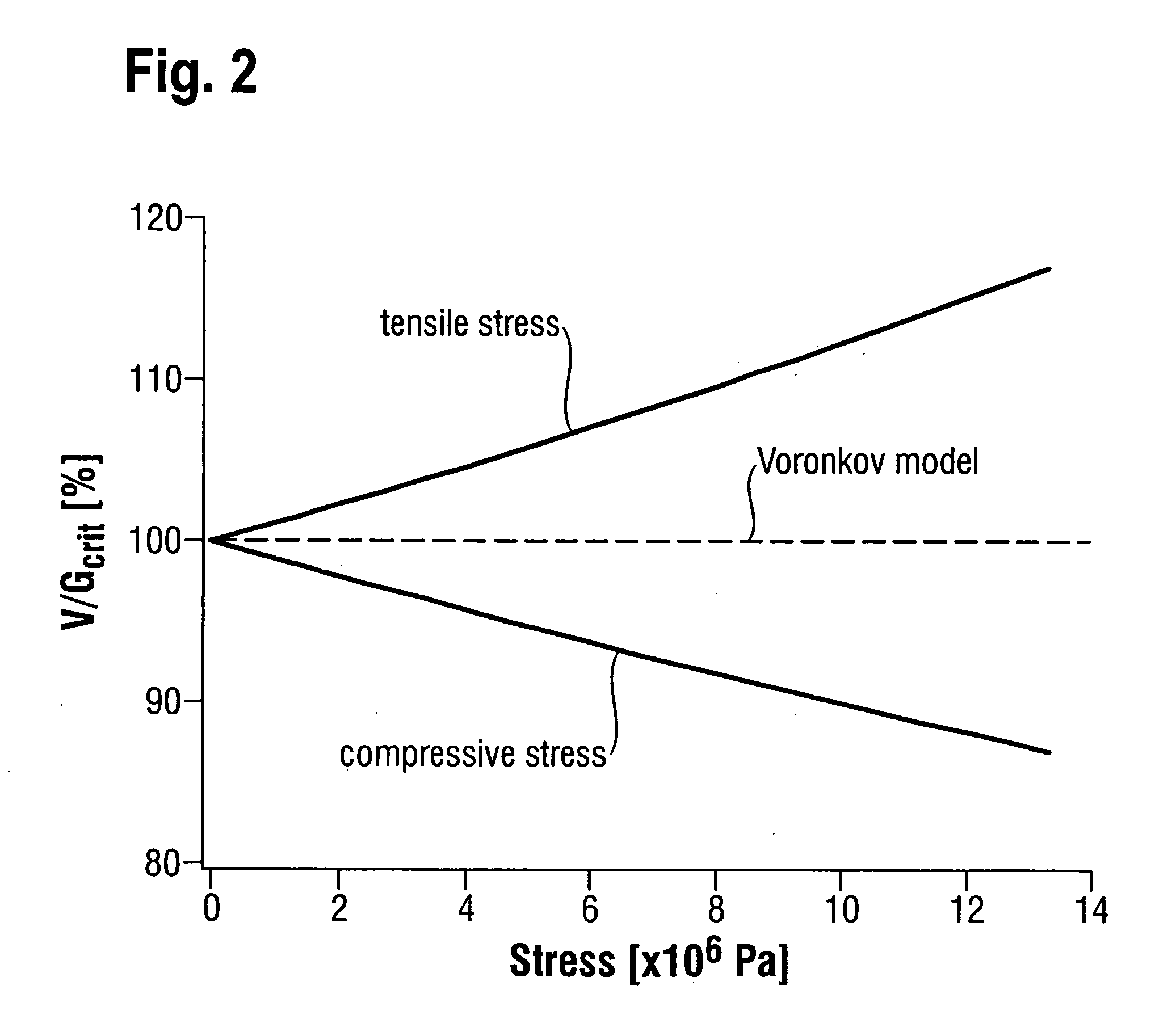
[0046]A map, which reveals thermomechanical stress fields in the single crystal, was compiled for this hot zone with the aid of simulation calculations. The aforementioned Flow Module program, which two-dimensionally calculates the elastic stresses a...


PUM

PropertyMeasurementUnit
diameteraaaaaaaaaa
sizeaaaaaaaaaa
temperatureaaaaaaaaaa

Abstract

Semiconductor wafers of silicon are produced by pulling a single crystal growing on a phase boundary from a melt contained in a crucible and cutting of semiconductor wafers therefrom, wherein during pulling of the single crystal, heat is delivered to a center of the phase boundary and a radial profile of a ratio V / G from the center to an edge of the phase boundary is controlled, G being the temperature gradient perpendicular to the phase boundary and V being the pull rate. The radial profile of the ratio V / G is controlled so that the effect of thermomechanical stress in the single crystal adjoining the phase boundary, is compensated with respect to creation of intrinsic point defects. The invention also relates to defect-free semiconductor wafers of silicon, which can be produced economically by this method.

Description

CROSS-REFERENCE TO RELATED APPLICATIONS[0001]This application claims the benefit of U.S. provisional application Ser. No. 60 / 887,847 filed Feb. 2, 2007 and claims priority to German application Serial No. 10 2007 005 346.2, filed Feb. 2, 2007. Both of these applications are herein incorporated by reference.BACKGROUND OF THE INVENTION[0002]1. Field of the Invention[0003]The invention relates to a method for producing semiconductor wafers of silicon, comprising pulling a single crystal growing on a phase boundary from a melt contained in a crucible and cutting semiconductor wafers from the pulled single crystal, wherein heat is delivered to a center of the phase boundary during pulling, and a radial profile of a ratio V / G from the center to an edge of the phase boundary is controlled, with G being the temperature gradient perpendicular to the phase boundary and V being the pull rate at which the single crystal is pulled from the melt. The invention also relates to defect-free semicond...

Claims


Application Information

Patent Timeline
Patent Type & Authority Applications(United States)
IPC IPC(8): B32B9/00H01L21/20
CPCC30B29/06C30B15/203H01L21/20
Inventor SATTLER, ANDREASVON AMMON, WILFRIEDWEBER, MARTINHAECKL, WALTERSCHMIDT, HERBERT
Owner SILTRONIC AG
Why Eureka
Try Eureka