Isolated transistor

a transistor and isolation technology, applied in the field of isolation transistors, can solve the problems of difficult current sensing, inability to facilitate complete electrical isolation, and inability to facilitate electrical isolation of its fabricated devices, and achieve the effect of reducing charging and other time-dependent surface-related phenomena

Inactive Publication Date: 2008-08-14
ADVANCED ANALOGIC TECHNOLOGIES INCORPORATED
View PDF41 Cites 114 Cited by
  • Summary
  • Abstract
  • Description
  • Claims
  • Application Information

AI Technical Summary

Benefits of technology

[0031]FIGS. 9A-9D illustrate cross-sectional views of termination structures for controlling su

Problems solved by technology

While both LOCOS and trench isolation can prevent unwanted surface conduction between devices, they do not facilitate complete electrical isolation.
Although conventional CMOS wafer fabrication offers high density transistor integration, it does not facilitate compete electrical isolation of its fabricated devices.
This restriction is substantial, preventing the use of the NMOS as a high-side switch, an analog pass transistor, or as a bidirectional switch.
It also makes current sensing more difficult and often precludes the use of integral source-body shorts needed to make the NMOS more avalanche rugged.
Moreover since the P-type substrate in a conventional CMOS is normally biased to the most negative on-chip potential (defined as “ground”), every NMOS is necessarily subjected to unwanted substrate noise.
While not as ideal as dielectric isolation, where oxide surrounds each device or circuit, junction isolation has historically offered the best compromise between manufacturing cost and isolation performance.
Growth of epitaxial layers is slow and time consuming, representing the single most expensive step in semiconductor wafer fabrication.
The isolation diffusion is also expensive, performed using high temperature diffusion for extended durations (up to 18 hours).
Prior to epitaxial growth however, this NBL layer must be diffused sufficiently deep to reduce its surface concentration, or otherwise the concentration control of the epitaxial growth will be adversely impacted.
Because the NBL is comprised of a slow diffuser, this pre-epitaxy diffusion process can take more than ten hours.
Only afte

Method used


Image

  • Isolated transistor
  • Isolated transistor
  • Isolated transistor

Examples


Embodiment Construction

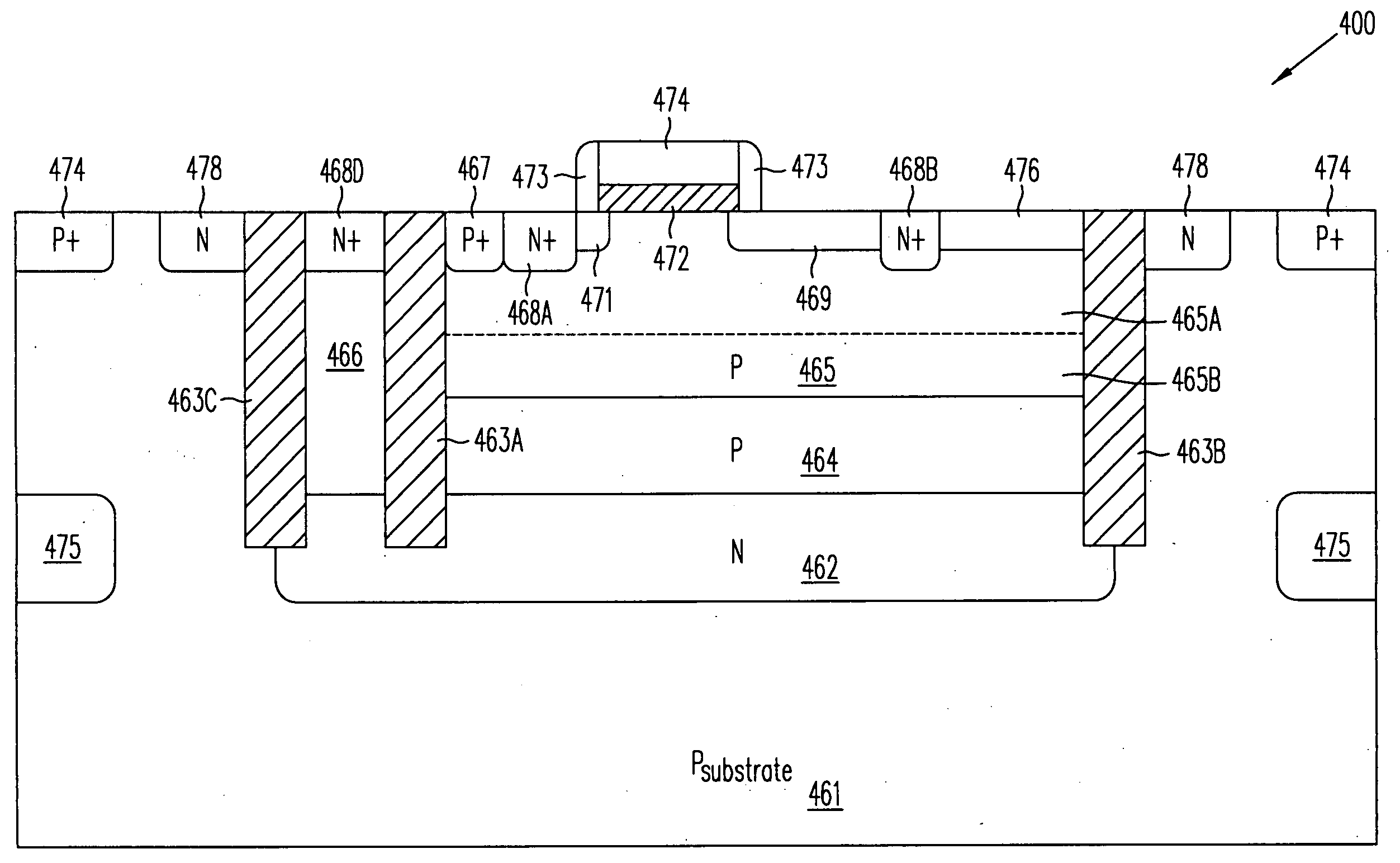
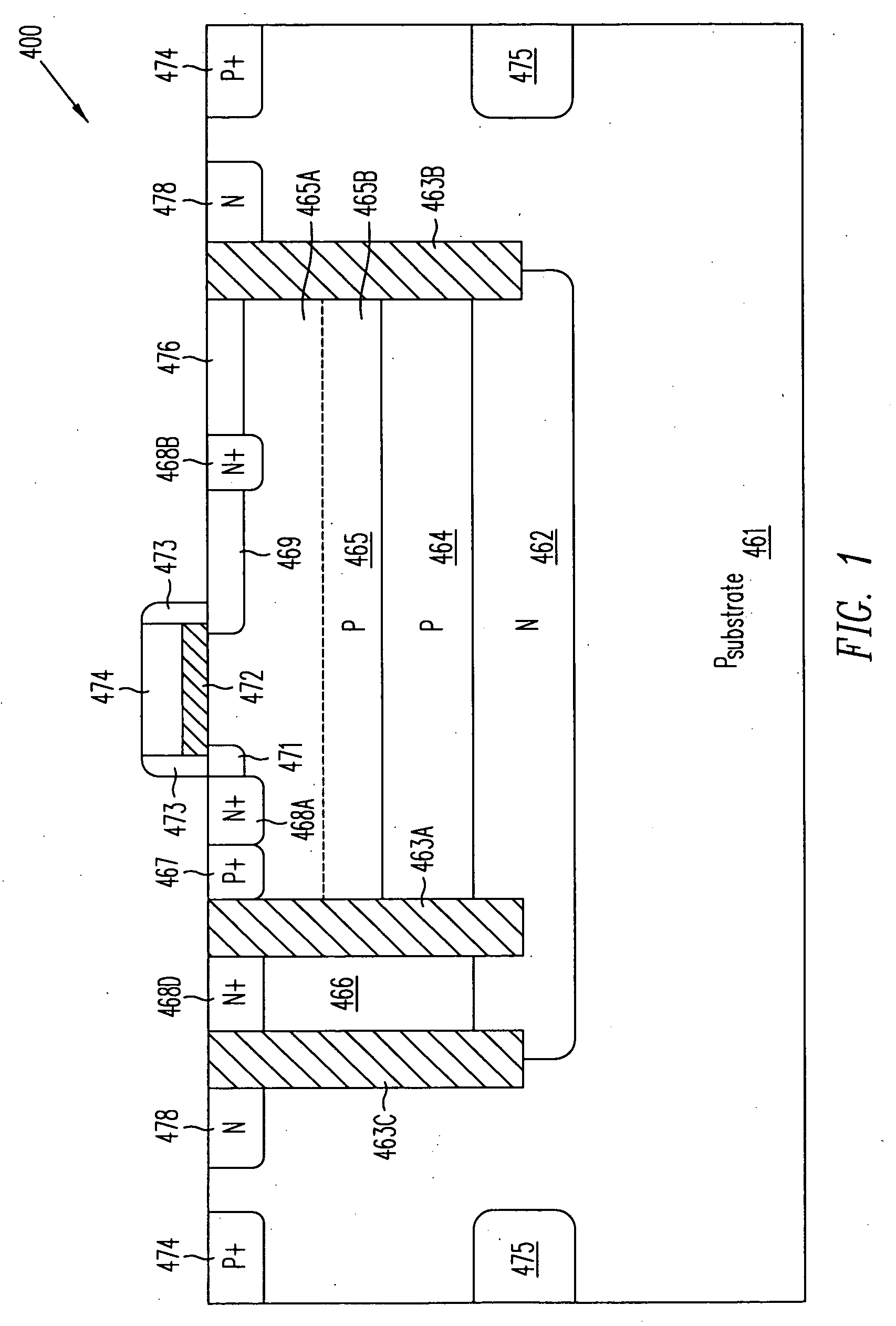
[0032]FIG. 1 illustrates a schematic cross-section of a fully isolated N-channel lateral DMOS (LDMOS) 400 made in accordance with this invention and fabricated without the need for epitaxial deposition or high temperature diffusions. The LDMOS 400 is fabricated in isolated P-type region 464. P-type region 464 and the lateral DMOS 400 fabricated within P-type region 464 are isolated from P-type substrate 461 by high-energy implanted N-type floor isolation region 462 and dielectric-filled trenches 463A and 463B.

[0033]The N-channel LDMOS 400 comprises: N+ drain region 468B, spaced from gate 474 by implanted N-type lightly-doped drain (LDD) region 469 and spaced from trench 463B by LDD 476 region, gate 474, preferably comprising polysilicon and / or silicide, gate oxide layer 472, N+ source region 468A, P+ body contact region 467 contacting a P-type well 465 comprising the body region of LDMOS 400. P-type well 465 may include at least an upper portion 465A and a lower portion 465B or any ...


PUM


Abstract

Various integrated circuit devices, in particular a transistor, are formed inside an isolation structure which includes a floor isolation region and a trench extending from the surface of the substrate to the floor isolation region. The trench may be filled with a dielectric material or may have a conductive material in a central portion with a dielectric layer lining the walls of the trench. Various techniques for terminating the isolation structure by extending the floor isolation region beyond the trench, using a guard ring, and a forming a drift region are described.

Description

CROSS-REFERENCE TO RELATED APPLICATIONS[0001]This application is a continuation-in-part of application Ser. No. ______ [Attorney Docket No. AATI-23A-DS-US], filed Feb. 14, 2008.[0002]This application is a continuation-in-part of application Ser. No. 11 / 890,993, filed Aug. 8, 2007. Application Ser. No. 11 / 890,993 is a continuation of application Ser. No. 11 / 444,102, filed May 31, 2006, and a continuation-in-part of the following applications:(a) application Ser. No. 10 / 918,316, filed Aug. 14, 2004, which is a divisional of application Ser. No. 10 / 218,668, filed Aug. 14, 2002, now U.S. Pat. No. 6,900,091, and(b) application Ser. No. 11 / 204,215, filed Aug. 15, 2005, which is a divisional of application Ser. No. 10 / 218,678, filed Aug. 14, 2002, now U.S. Pat. No. 6,943,426.Each of the foregoing applications and patents is incorporated herein by reference in its entirety.BACKGROUND OF THE INVENTION[0003]In the fabrication of semiconductor integrated circuit (IC) chips, it is frequently ne...

Claims


Application Information

Patent Timeline
IPC IPC(8): H01L29/78
CPCH01L21/26586H01L29/0615H01L2924/0002H01L29/0626H01L29/063H01L29/0638H01L29/0653H01L29/0661H01L29/086H01L29/1045H01L29/105H01L29/1083H01L29/1087H01L29/41766H01L29/7809H01L29/7835H01L29/808H01L29/8613H01L29/866H01L2924/00H01L29/7811H01L29/7816H01L29/7824
Inventor DISNEY, DONALD R.WILLIAMS, RICHARD K.
Owner ADVANCED ANALOGIC TECHNOLOGIES INCORPORATED
Why Eureka
Try Eureka