

Organometallic precursors for seed/barrier processes and methods thereof
a technology of organic precursors and barriers, applied in the direction of coatings, chemical vapor deposition coatings, metallic material coating processes, etc., can solve the problems of increasing the resistivity and rc delay and reducing the resistance of the electrical lin
- Summary
- Abstract
- Description
- Claims
- Application Information
AI Technical Summary
Benefits of technology
Problems solved by technology
Method used
Image

Examples
Embodiment Construction
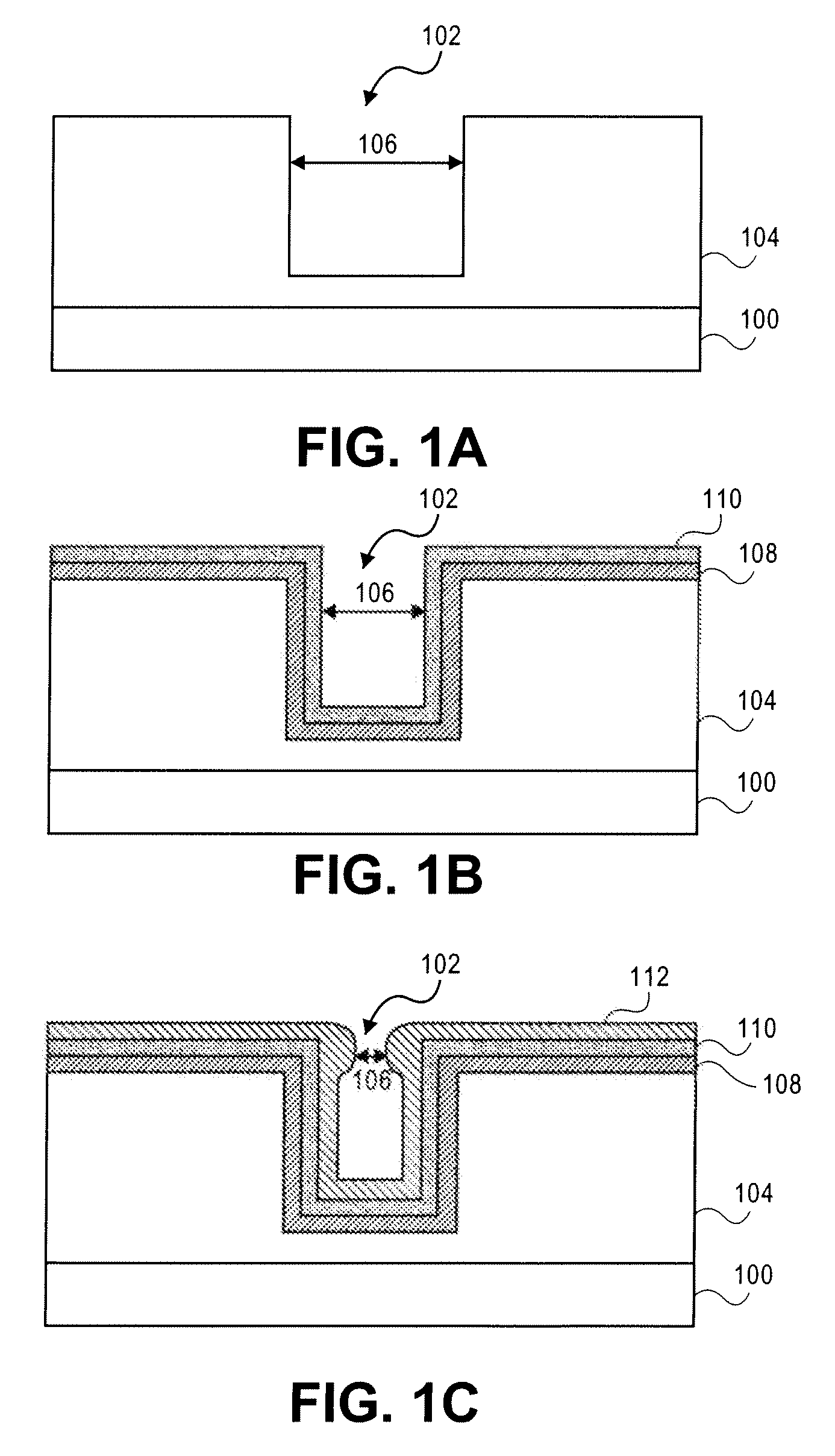
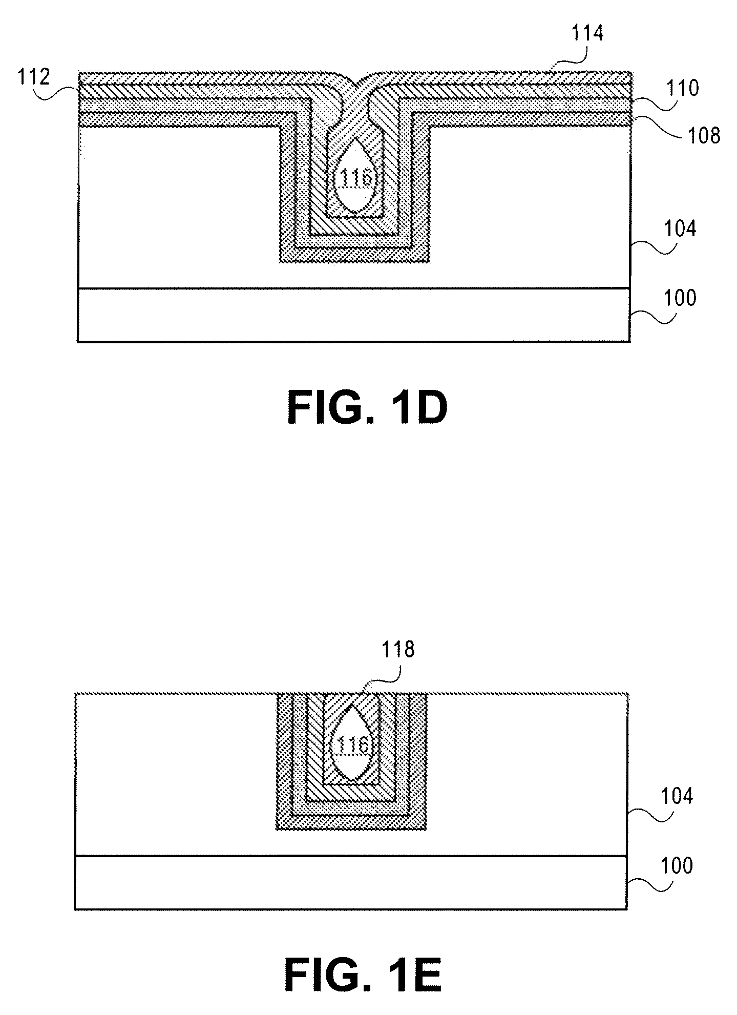
[0013]FIGS. 1A to 1E illustrate a damascene process for fabricating copper interconnects on a semiconductor wafer. FIG. 1A illustrates a substrate 100, such as a semiconductor wafer, which includes a trench 102 that has been etched into a dielectric layer 104. The trench 102 includes a gap 106 through which metal may enter during metallization processes.
[0014]FIG. 1B illustrates the trench 102 after a conventional barrier layer 108 and a conventional adhesion layer 110 have been deposited thereon. The barrier layer 108 prevents copper metal from diffusing into the dielectric layer 104. The adhesion layer 110 enables copper metal to become deposited onto the barrier layer 108. The barrier layer 108 is generally formed using a material such as tantalum nitride (TaN) and is deposited using a PVD process. The barrier layer 108 may be around 10 Angstroms (Å) to 10 nanometers (nm) thick, although it is generally around 5 nm thick. The adhesion layer 110 is generally formed using a metal s...
PUM
| Property | Measurement | Unit |
|---|---|---|
| thick | aaaaa | aaaaa |
| thick | aaaaa | aaaaa |
| thick | aaaaa | aaaaa |
Abstract
Description
Claims
Application Information