Surface-Emission Laser Diode and Fabrication Process Thereof

a laser diode and laser diode technology, applied in lasers, semiconductor devices, semiconductor lasers, etc., can solve the problems of increasing the demand for output, and achieve the effects of excellent high temperature characteristics, large gain, and large outpu

Active Publication Date: 2008-09-04
RICOH KK
View PDF13 Cites 58 Cited by
  • Summary
  • Abstract
  • Description
  • Claims
  • Application Information

AI Technical Summary

Benefits of technology

[0147]With the surface-emission laser diode of the present invention having the wavelength of 680 nm or longer, a large gain is attained for the active layer and it is possible to provide a large output. Further, the surface-emission laser diode of the present invention has excellent high temperature characteristics. Thus, by using such a surface-emission laser diode, it is possible to achieve, in spite of the fact there is an increase of absorption loss by the fiber, optical transmission of short range. Thus, an economical high-speed optical transmission module or an optical transceiver module that combines a low cost POF with a low cost optical source of surface-emission laser diode is realized. Further, an optical communication system that uses these is realized. Because such an optical communicating system is extremely economical, it is suited for the optical communication systems of home use, or for use in office rooms, or for the use inside an apparatus.

Problems solved by technology

Thus, there are many cases in which demand of increased output is imposed to such surface-emission laser diodes.

Method used


Image

  • Surface-Emission Laser Diode and Fabrication Process Thereof
  • Surface-Emission Laser Diode and Fabrication Process Thereof
  • Surface-Emission Laser Diode and Fabrication Process Thereof

Examples


example 1

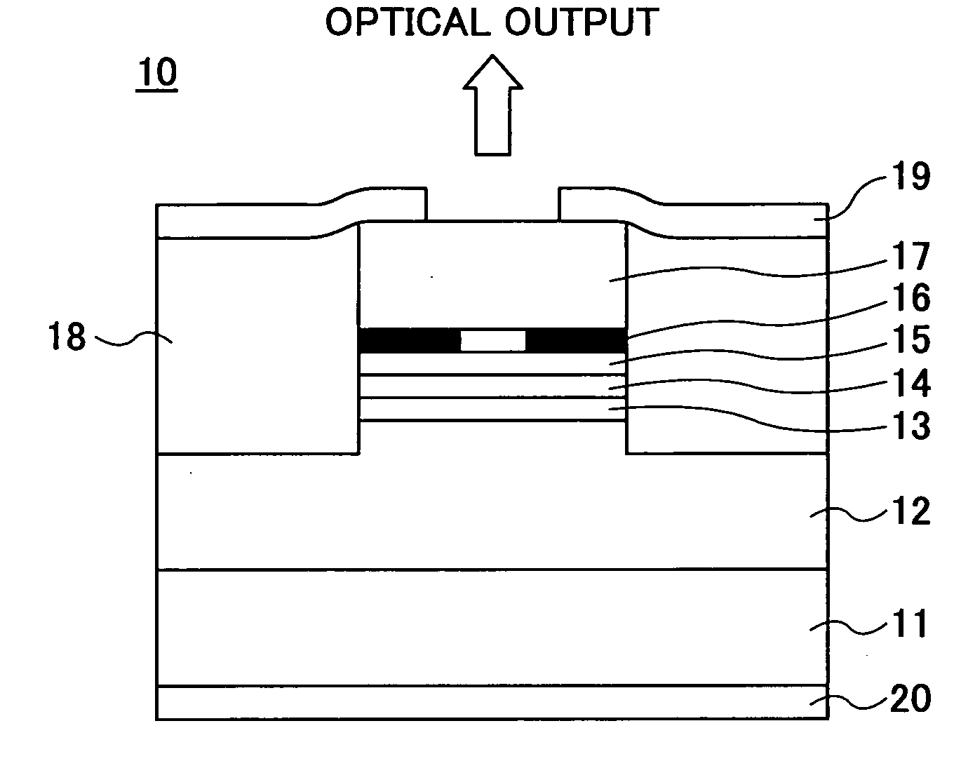
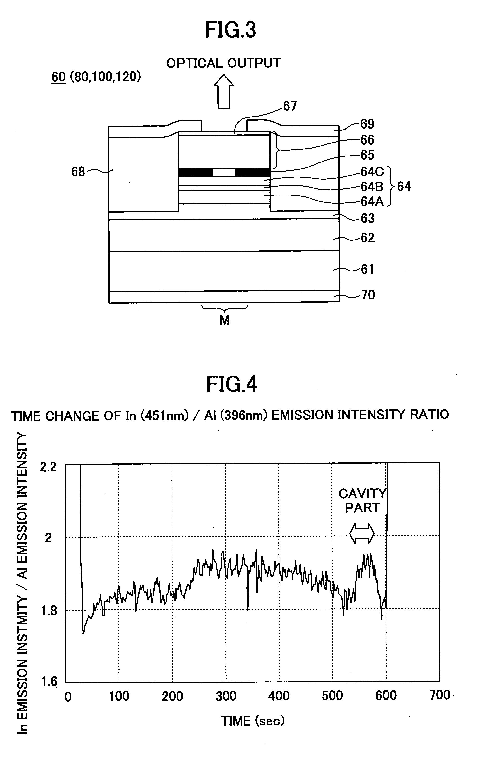
[0253]FIG. 3 shows the construction of a surface-emission laser diode 60 according to Example 1 of the present invention. It should be noted that the surface-emission laser diodes of Examples 2, 3 and 4 to be described later have also the construction similar to that of FIG. 3.

[0254]Referring to FIG. 3, Example 1 forms a VCSEL stacked structure on an n-GaAs monocrystal (100) substrate 61 by consecutively stacking, by way of an MOCVD process, a first lower semiconductor DBR 62 in which an n-AlAs / Al0.3Ga0.7As pair is repeated for 42.5 times, a second lower semiconductor DBR 63 in which an n-Al0.95Ga0.05As / Al0.3Ga0.7As pair is repeated six times, a Ga0.5In0.5P lower spacer layer 64A, a GaInAsP / Ga0.5In0.5P (well / barrier) TQW active layer 64B, a Ga0.5In0.5P upper spacer layer 64C, a p-AlAs selective oxidation layer 65, an upper semiconductor DBR 66 in which a p-Al0.95Ga0.05As / Al0.3Ga0.7As pair is repeated 34.5 times, and a p-GaAs contact layer 67. Here, the lower spacer layer 64A, the ac...

example 2

[0263]Next, a surface-emission laser diode 80 according to Example 2 of the present invention will be explained. As noted before, the surface-emission laser diode 80 of Example 2 has a construction similar to that of FIG. 3.

[0264]Referring to FIG. 3, Example 2 forms a VCSEL stacked structure on an n-GaAs monocrystal (100) substrate 61 by consecutively stacking, by way of an MOCVD process, a first lower semiconductor DBR 62 in which an n-AlAs / Al0.5Ga0.5As pair is repeated for 47.5 times, a second lower semiconductor DBR 63 in which an n-Al0.95Ga0.05As / Al0.5Ga0.5As pair is repeated ten times, a (Al0.5Ga0.5)0.5In0.5P lower spacer layer 64A, an In0.46Ga0.54P / (Al0.5Ga0.5)0.5In0.5P (well / barrier) TQW active layer 64B, a (Al0.5Ga0.5)0.5In0.5P upper spacer layer 64C, a p-AlAs selective oxidation layer 65, an upper semiconductor DBR 66 in which a p-Al0.95Ga0.05As / Al0.5Ga0.5As pair is repeated 40.5 times, and a p-GaAs contact layer 67.

[0265]Next, a circular mesa mask is patterned on such a VC...

example 3

[0271]Next, a surface-emission laser diode 100 according to Example 3 of the present invention will be explained. As noted before, the surface-emission laser diode 100 of Example 3 has a construction similar to that of FIG. 3.

[0272]Referring to FIG. 3, Example 3 forms a VCSEL stacked structure on an n-GaAs monocrystal (100) substrate 61 by consecutively stacking, by way of an MOCVD process, a first lower semiconductor DBR 62 in which an n-AlAs / Al0.5Ga0.5As pair is repeated for 40.5 times, a second lower semiconductor DBR 63 in which an n-Al0.95Ga0.05As / Al0.15Ga0.85As pair is repeated five times, an In0.27Ga0.73As0.44P0.56 lower spacer layer 64A, an GaAs / In0.27Ga0.73As0.44P0.56 (well / barrier) TQW active layer 64B, an In0.27Ga0.73As0.44P0.56 upper spacer layer 64C, a p-AlAs selective oxidation layer 65, an upper semiconductor DBR 66 in which a p-Al0.95Ga0.05As / Al0.15Ga0.85As pair is repeated 30.5 times, and a p-GaAs contact layer 67.

[0273]Next, mesa etching is conducted to the VCSEL s...


PUM


Abstract

A surface-emission laser diode comprises a cavity region over a semiconductor substrate and includes an active layer containing at least one quantum well active layer producing a laser light and a barrier layer, a spacer layer is provided in the vicinity of the active layer and formed of at least one material, an upper and lower reflectors are provided at a top part and a bottom part of the cavity region, the cavity region and the upper and lower reflectors form a mesa structure over the semiconductor substrate, the upper and lower reflectors being formed of a semiconductor distributed Bragg reflector having a periodic change of refractive index and reflecting incident light by interference of optical waves, at least a part of the semiconductor distributed Bragg reflector is formed of a layer of small refractive index of AlxGa1-xAs (0<x≦1) and a layer of large refractive index of AlyGa1-yAs (0≦y<x≦1), the lower reflector is formed of a first lower reflector having a low-refractive index layer of AlAs and a second lower reflector formed on the first lower reflector, the second lower reflector has a low-refractive index layer of AlGaAs, any one layer constituting the cavity region contains In.

Description

TECHNICAL FIELD[0001]The present invention relates to surface-emission laser diodes and the fabrication process thereof.BACKGROUND ART[0002]A surface-emission laser diode (surface-emission semiconductor laser) is a laser diode that emits light in a vertical direction to the substrate and is used for civil purposes, such as optical source of optical telecommunication including optical interconnection, optical source of optical pickup devices, optical source of image forming apparatuses, and the like.[0003]Patent Reference 1 Japanese Laid-Open Patent Application 2002-164621[0004]Patent Reference 2 Japanese Laid-Open Patent Application 9-107153 official gazette[0005]Patent Reference 3 Japanese Laid-Open Patent Application 2001-60739[0006]Patent Reference 4 Japanese Laid Open Patent Application 2001-168461[0007]Non-patent Reference 1 IEEE Photonics Technology Letters, Vol. 10, No. 12, pp. 1676-1678, 1998 (Tokyo Institute of Technology)[0008]Non-patent Reference 2 IEEE Photonics Technolo...

Claims


Application Information

Patent Timeline
Patent Type & Authority Applications(United States)
IPC IPC(8): H01S5/187H01L33/00H01S5/042H01S5/183H01S5/22H01S5/42
CPCH01S5/02284H01S5/0425H01S5/18311H01S5/343H01S5/18383H01S5/2205H01S5/423H01S5/18347H01S5/04256H01S5/02251
Inventor SATO, SHUNICHIITOH, AKIHIROJIKUTANI, NAOTO
Owner RICOH KK
Why Eureka
Try Eureka