Photonic crystal light emitting device using photon-recycling

a photonic crystal and light-emitting technology, applied in the field of light-emitting devices, can solve the problems of difficult improvement over conventional corrugated interface surfaces (cis) or surface roughness structures, serious damage to semiconductor crystal structures for electrical operation,

Active Publication Date: 2008-09-11
SAMSUNG ELECTRONICS CO LTD
View PDF4 Cites 60 Cited by
  • Summary
  • Abstract
  • Description
  • Claims
  • Application Information

AI Technical Summary

Benefits of technology

[0012]An aspect of the present invention provides a photonic crystal light emitting device capable of more fully using merits of a photonic crystal structure such as light e...

Problems solved by technology

However, due to a dry etching generally used to form a photonic crystal structure, a serious damage occurs in a semiconductor crystal structure for electrical operation.
The photonic crystal LED having such a structure is incapable of utilizing intensification of internal quantum efficiency that is one of greatest characteristics of a photonic crystal.
Accordingly, it is difficult to provide improvement over conventional corrugated interface surface (CIS) or surface roughness structures.
However, this is a conclusion without fully considering that an LED is electrically driven.
Due to a dry etching generally used to form the holes H having the depth, particularly, inductive coupling plasma reactive ion etching (ICPRIE), a serious damage occurs in a semiconductor crystal structure for electrical operations, particularly, a crystal structure around an active layer.
Due to this...

Method used


Image

  • Photonic crystal light emitting device using photon-recycling
  • Photonic crystal light emitting device using photon-recycling
  • Photonic crystal light emitting device using photon-recycling

Examples


Embodiment Construction

[0034]Exemplary embodiments of the present invention will now be described in detail with reference to the accompanying drawings. The invention may however be embodied in many different forms and should not be construed as limited to the embodiments set forth herein. Rather, these embodiments are provided so that this disclosure will be thorough and complete, and will fully convey the scope of the invention to those skilled in the art. In the drawings, the shapes and dimensions may be exaggerated for clarity, and the same reference numerals are used throughout to designate the same or similar components.

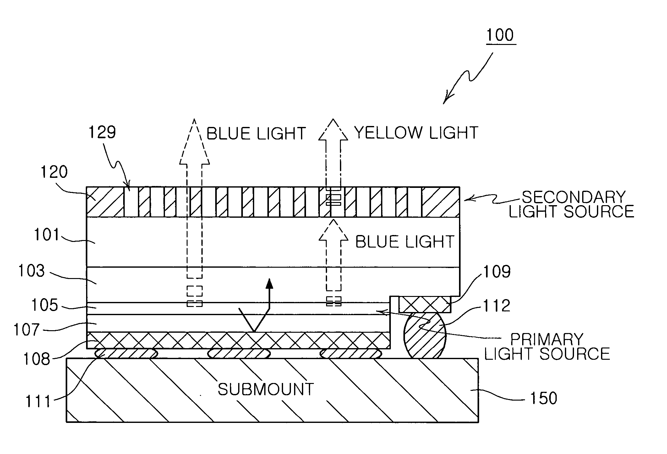
[0035]FIG. 4 is across-sectional view illustrating a photonic crystal light emitting device 100 according to an embodiment of the present invention. FIG. 4, particularly, illustrates the photonic crystal light emitting device 100 having a flip-chip structure where a chip is mounted on an Si submount 150 while turned upside down in such a way that a transparent sapphire substrate 101 ...


PUM


Abstract

A photonic crystal light emitting device including: a light emitting diode (LED) light emitting structure including a first conductive semiconductor layer, a second conductive semiconductor layer, and an active layer interposed between the first and second conductive semiconductor layers; and a first photon-recycling light emitting layer formed on one surface of the first conductive semiconductor layer, opposite to the active layer, wherein the first photon-recycling light emitting layer absorbs a primary light emitted from the LED light emitting structure and emits a light having a different wavelength from that of the primary light, and a photonic crystal structure is formed on an entire thickness of the first photon-recycling light emitting layer.

Description

CROSS-REFERENCE TO RELATED APPLICATIONS[0001]This application claims the priority of Korean Patent Application No. 2007-0021432 filed on Mar. 5, 2007, in the Korean Intellectual Property Office, the disclosure of which is incorporated herein by reference.BACKGROUND OF THE INVENTION[0002]1. Field of the Invention[0003]The present invention relates to a light emitting device, and more particularly, to a photonic crystal light emitting device with high optical efficiency using photon-recycling.[0004]2. Description of the Related Art[0005]Recently, there is performed a lot of researches on applying a photonic crystal structure as technologies to improve light extraction efficiency of semiconductor light emitting device such as GaN-based light emitting diodes (LEDs). LEDs having a photonic crystal structure may have merits of not only improving light extraction efficiency but also improving internal quantum efficiency and controlling a light emitting direction.[0006]However, due to a dry...

Claims


Application Information

Patent Timeline
IPC IPC(8): H01L33/00H01L33/20H01L33/46H01L33/50
CPCH01L33/20H01L33/46H01L2933/0083H01L33/508H01L33/502H01L2224/14
Inventor KIM, HYUN JUNCHOI, CHANG HWANMOON, WON HALEE, JONG HOYONG, JAE CHULKIM, JIN HA
Owner SAMSUNG ELECTRONICS CO LTD
Why Eureka
Try Eureka