Highly selective liners for semiconductor fabrication

a technology of selective etching and liners, which is applied in the direction of semiconductor devices, semiconductor/solid-state device details, electrical devices, etc., can solve the problems of only feasible “over-etching” steps, unintentional etching of underlying layers, and unintentional etching of materials and layers underneath the selective etching step, etc., to achieve greater protection, reduce the risk of etching, and reduce the resistance of trench liner materials

Active Publication Date: 2008-09-11
TEXAS INSTR INC
View PDF1 Cites 6 Cited by
  • Summary
  • Abstract
  • Description
  • Claims
  • Application Information

AI Technical Summary

Benefits of technology

[0018]The invention relates to an isolation structure for isolating active regions on a semiconductor device and related fabrication methods. In one aspect of the invention, the isolation structure described herein differs from conventional isolation structures by the use of a trench liner material that exhibits a comparative resistance to the etch solution that is used to remove the planarization stop used on the active region. This comparative resistance results in a slower rate of etching of the trench liner material than of the active region planarization stop material, thereby allowing greater protection against accidental etching into and damage of the isolation trench. If the etch rate difference is sufficiently large, then the fabrication process may expressly “over-etch” the semiconductor by exposing it to the etch solution for a protracted period of time in order to ensure the complete removal of the active region planarization stop, while relying on the greater resistance of the trench liner material to protect the isolation trench. Thus, this aspect of the invention provides more precise control over the fabrication process and results in a higher manufacturing quality standard for semiconductor devices.
[0019]In another aspect of the invention, the isolation structure described herein exerts a greater tensile strain on the active regions that may improve performance in NMOS devices formed upon an active region. As discussed hereinabove, conventional trench liners are known to exert a tensile stress of 400-600 MPa on the active regions of the semiconductor. Other materials are known to exhibit a greater tensile strain if deposited in the isolation trench, which provides for enhanced carrier mobility and a higher-performance transistor.

Problems solved by technology

A common problem with this selective deposition technique is the risk of unintentionally etching the materials and layers underneath the layer that is being selectively etched.
This may occur if the underlying material is sensitive to the etching solution used for etching the selectively deposited layer atop it; in this case, the underlying layer may be unintentionally etched during the etching step.
This “over-etching” step is only feasible because the comparative insensitivity of the etch-stop layer to the etching solution protects the underlying materials from unintended exposure to the etching solution.

Method used


Image

  • Highly selective liners for semiconductor fabrication
  • Highly selective liners for semiconductor fabrication
  • Highly selective liners for semiconductor fabrication

Examples


Embodiment Construction

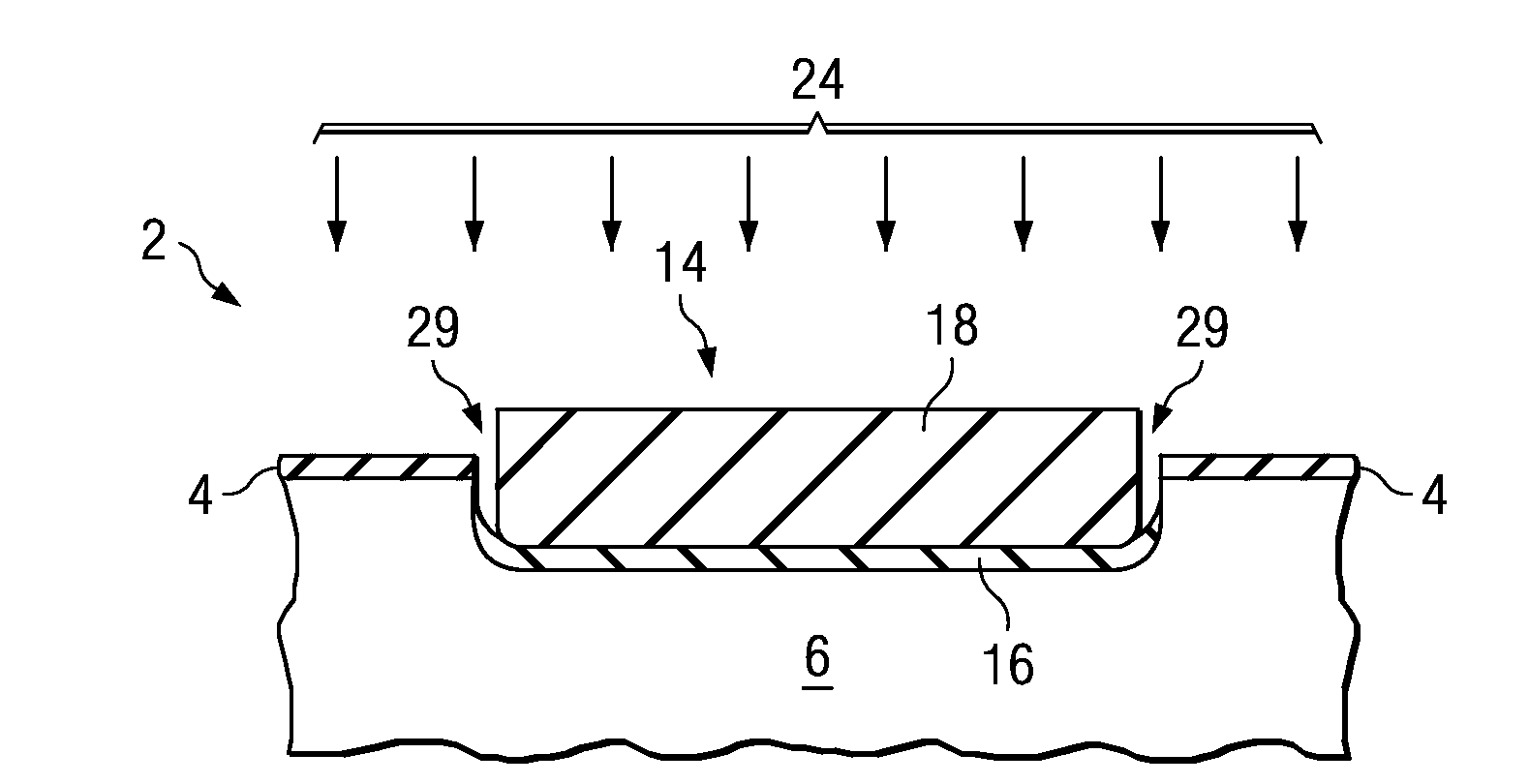
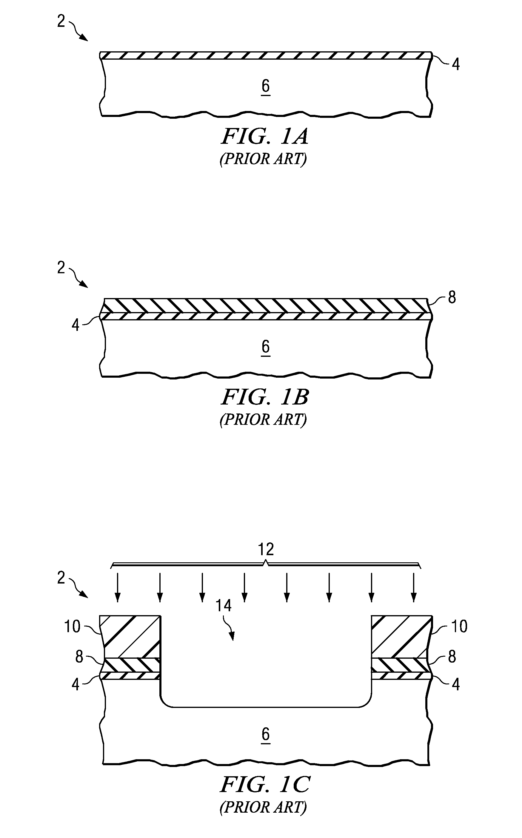
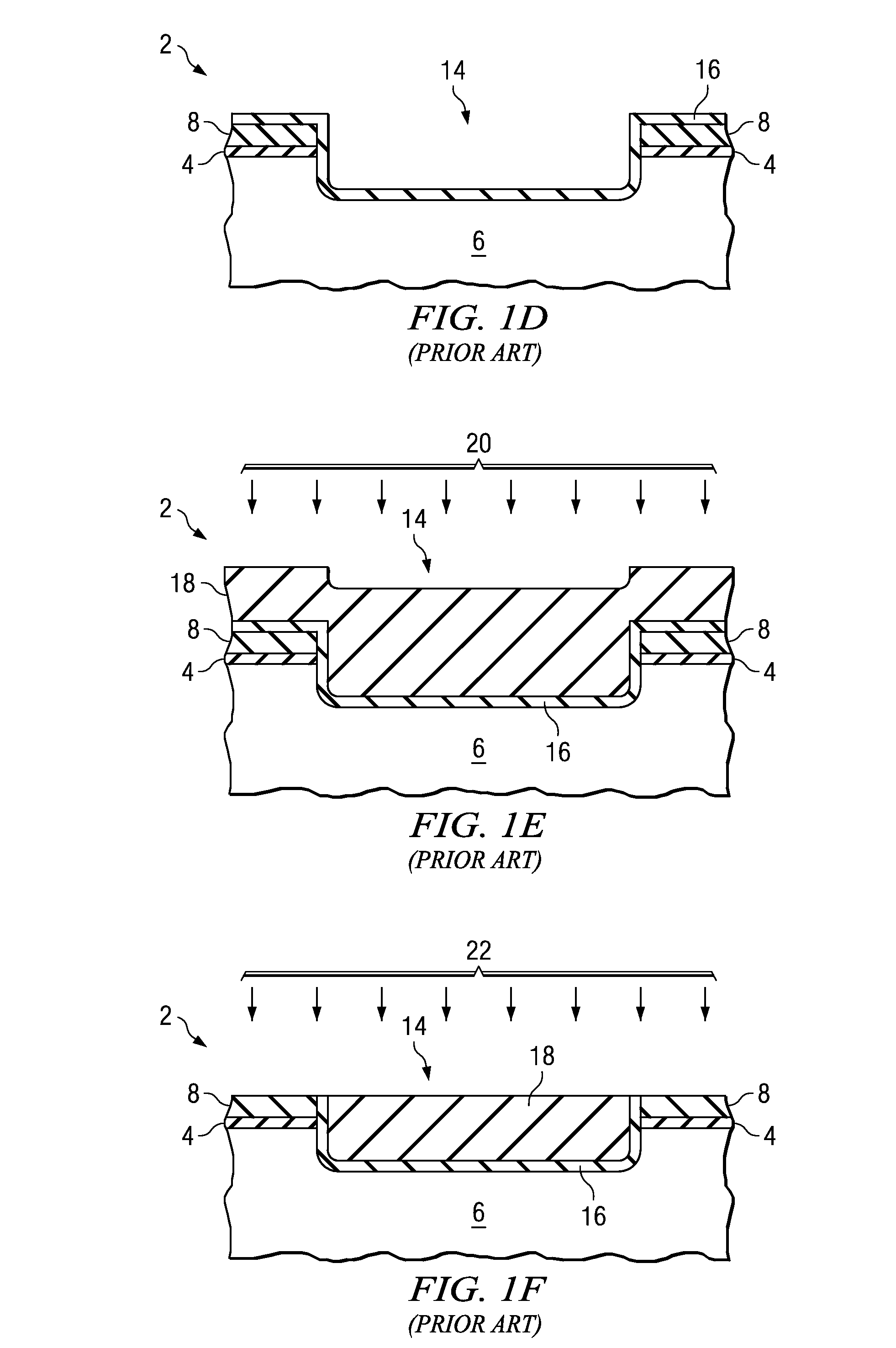
[0029]One or more aspects of the present invention are described with reference to the drawings, wherein like reference numerals are generally utilized to refer to like elements throughout, and wherein the various structures are not necessarily drawn to scale. In the following description, for purposes of explanation, numerous specific details are set forth in order to provide a thorough understanding of one or more aspects of the present invention. It may be evident, however, to one skilled in the art that one or more aspects of the present invention may be practiced with a lesser degree of these specific details. In other instances, well-known structures and devices are shown in block diagram form in order to facilitate describing one or more aspects of the present invention.

[0030]The inventors of the present invention discovered a problem associated with conventional trench isolation processing. More particularly, it was discovered that during the removal of the nitride that serv...


PUM

PropertyMeasurementUnit
tensile stressaaaaaaaaaa
dielectricaaaaaaaaaa
tensile strainaaaaaaaaaa

Abstract

A method for manufacturing an isolation structure is disclosed that protects the isolation structure during etching of a dichlorosilane (DCS) nitride layer. The method involves the formation of a bis-(t-butylamino)silane-based nitride liner layer within the isolation trench, which exhibits a five-fold greater resistance to nitride etching solutions as compared with DCS nitride, thereby allowing protection against damage from unintended over-etching. The bis-(t-butylamino)silane-based nitride layer also exerts a greater tensile strain on moat regions that results in heightened carrier mobility of active regions, thereby increasing the performance of NMOS transistors embedded therein.

Description

CROSS REFERENCE TO RELATED APPLICATIONS[0001]This patent application claims the benefit for priority under 35 U.S.C. 119(e) of U.S. Provisional Patent Application No. 60 / 877,302 (“Highly Selective Liners for Semiconductor Fabrication”), filed on Dec. 27, 2006, which is incorporated by reference as if fully rewritten herein.FIELD[0002]The present disclosure relates generally to the fabrication of semiconductor devices, and more particularly to materials used as liners in the process of manufacturing semiconductor devices.BACKGROUND[0003]Integrated semiconductor circuits are built through a very intricate process of creating and interconnecting, on a silicon wafer, a plurality of devices comprised of layers of chemicals with various electromechanical properties. The steps for producing such devices are discussed herein as background for the discussion of the invention.[0004]The process begins with a silicon wafer and the designation of doped moat areas, where NMOS and PMOS devices are...

Claims


Application Information

Patent Timeline
Patent Type & Authority Applications(United States)
IPC IPC(8): H01L29/78H01L21/762H01L21/336H01L23/58
CPCH01L21/76224H01L29/7846H01L21/823878H01L21/823807
Inventor MEHTA, NARENDRA SINGHBATHER, WAYNE ANTHONYVARGHESE, AJITH
Owner TEXAS INSTR INC
Why Eureka
Try Eureka