Transistor with Enhanced Channel Charge Inducing Material Layer and Threshold Voltage Control

Active Publication Date: 2010-12-30
THE UNITED STATES OF AMERICA AS REPRESENTED BY THE SECRETARY OF THE NAVY
View PDF8 Cites 126 Cited by
  • Summary
  • Abstract
  • Description
  • Claims
  • Application Information

AI Technical Summary

Benefits of technology

[0007]Various etch techniques can be used to etch the ECCIML with minimal altering the thickness of the BML. In certain embodiments using an AlN ECCIML over an AlGaN BML, an AZ-400K chemical etch process is used to remove the ECCIML layer and to expose the AlGaN BML with minimal altering of the thickness of the barrier material layer. The advantage of the use of AZ-400K chemical etch to remove the ECCIML layer is that the chemical can etch the AlN ECCIML but will have a very slow etch rate (high selectivity) for etching the AlGaN BML or GaN BML capping layer. In other embodiments, a GaN capping layer is formed on the ECCIML and a plasma etch process is used to remove at least a portion of the ECCIML before etching the ECCIML. The plasma etch process can be optimized to etch GaN at a higher etch rate than AlGaN. One advantage of the use of an GaN capping layer on the ECCIML is the GaN capping layer will minimize the lateral etch of the ECCIML in the case of poor adhesion of an etch protection layer such as silicon nitride on the surface of the ECCIML, and thus provide good lateral control of the ECCIML etch. A silicon nitride layer with poor adhesion can allow the chemical

Problems solved by technology

Shifting the threshold voltage to create an enhancement mode device has been attempted by etching AlGaN barrier material layer to be sufficiently thin to reduce the polarization induced two dimensional electron gas channel charge or by implanting negative charge in the AlGaN barrier material layer under the gate by exposing the device to a fluorine-based plasma, but plasma expos

Method used


Image

  • Transistor with Enhanced Channel Charge Inducing Material Layer and Threshold Voltage Control
  • Transistor with Enhanced Channel Charge Inducing Material Layer and Threshold Voltage Control
  • Transistor with Enhanced Channel Charge Inducing Material Layer and Threshold Voltage Control

Examples


Embodiment Construction

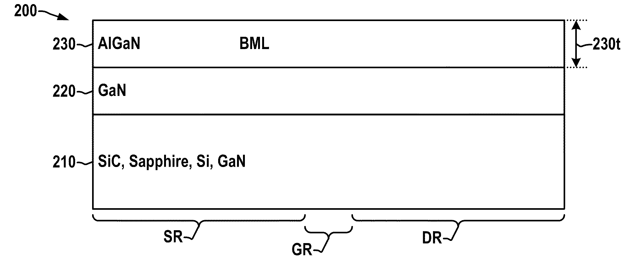
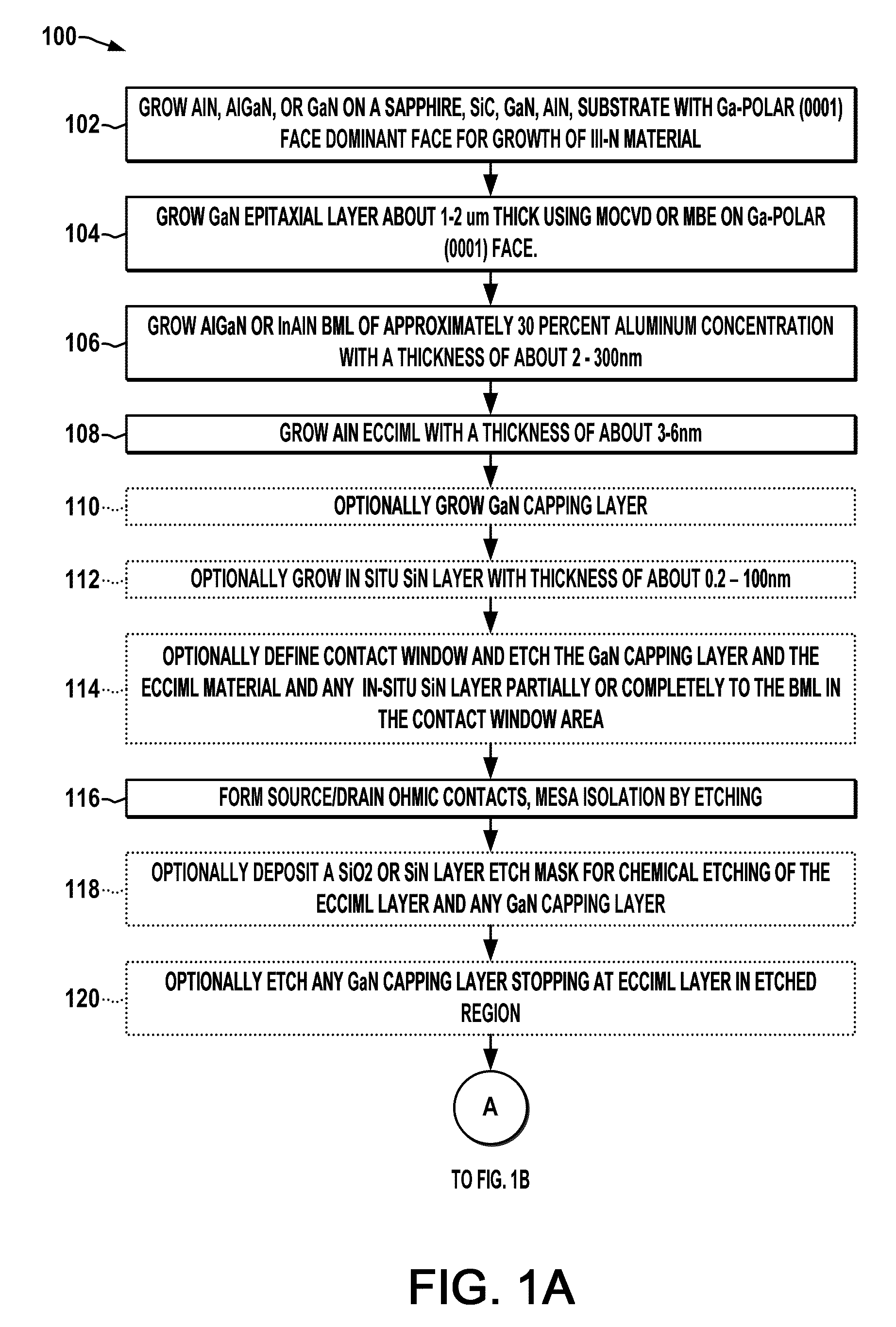
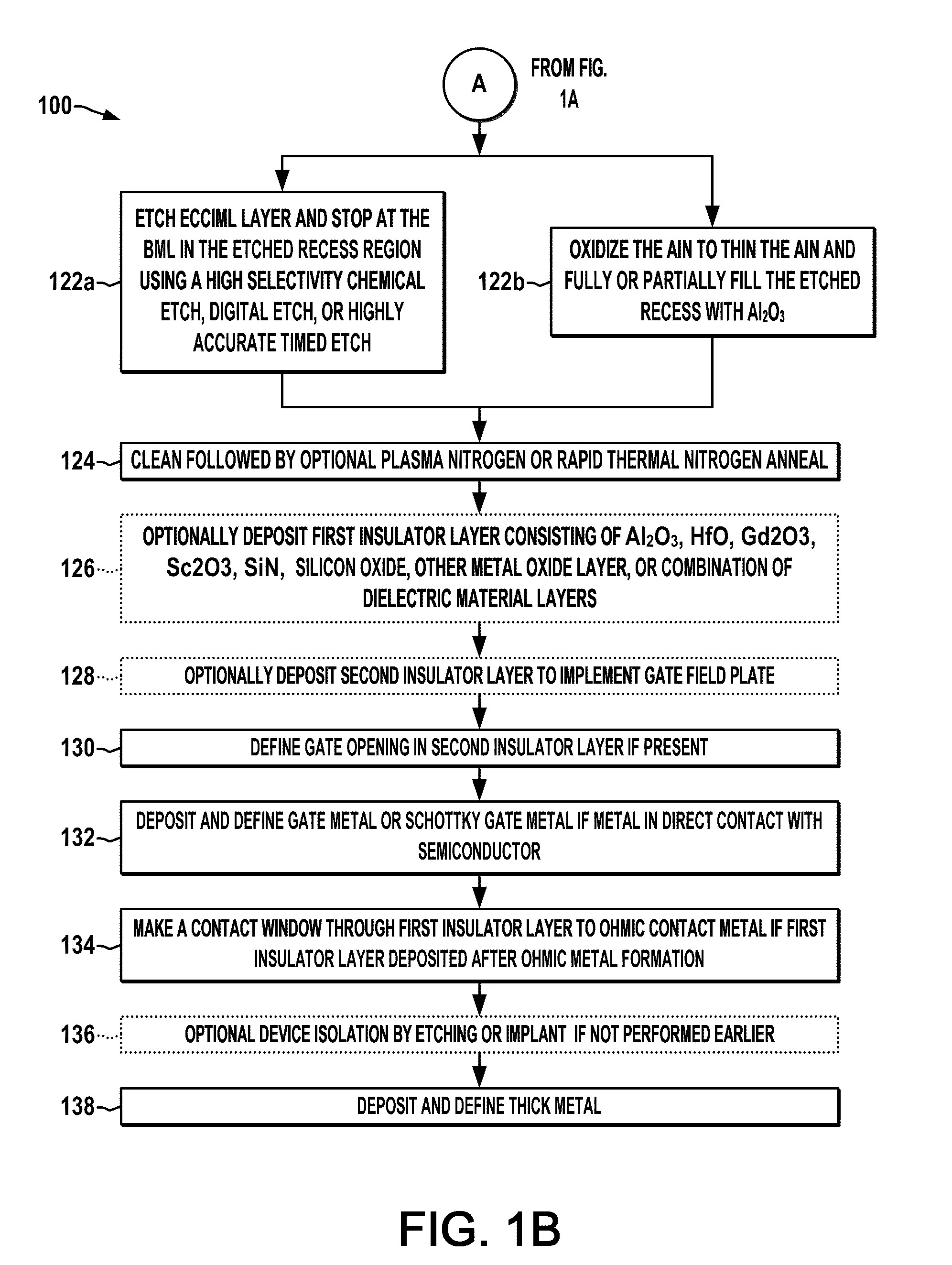
[0017]One or more embodiments or implementations are hereinafter described in conjunction with the drawings, where like reference numerals are used to refer to like elements throughout, and where the various features are not necessarily drawn to scale. The disclosure provides transistors and fabrication methods to facilitate precise, uniform, and repeatable FET threshold voltage control via control over the BML thickness, along with low source-drain access impedance through use of an enhanced channel charge inducing material layer (or layers) (ECCIML) in the source and drain access regions. The disclosure finds particular utility in connection with GaN, AlN, AlGaN, InGaN, InAlN, InAlGaN material systems having at least one heterojunction and either polar, semi-polar, or non-polar material, and the resulting transistors can be used for enhancement or depletion mode applications, including normally-off power switching devices with high mobility, enhancement mode transistors for enhanc...


PUM


Abstract

High electron mobility transistors and fabrication processes are presented in which a barrier material layer of uniform thickness is provided for threshold voltage control under an enhanced channel charge inducing material layer (ECCIML) in source and drain regions with the ECCIML layer removed in the gate region.

Description

REFERENCE TO RELATED APPLICATION[0001]This application claims priority to and the benefit of U.S. Provisional Patent Application Ser. No. 61 / 220,272, filed Jun. 25, 2009, entitled “Transistor with Enhanced Channel Charge Inducing Material Layer and Threshold Voltage Control”, the entirety of which is hereby incorporated by reference.FIELD OF THE DISCLOSURE[0002]The present disclosure relates generally to semiconductor devices and fabrication methods therefor, and in particular to high electron mobility transistors with a barrier material layer of uniform thickness for threshold voltage control beneath an enhanced channel charge inducing material layer in source and drain access regions with the enhanced channel charge inducing material layer removed in the gate region.BACKGROUND[0003]Wide-bandgap High Electron Mobility Transistors (HEMTs) offer thermal and chemical stability, as well as high mobility and breakdown field, but the standard HEMT is a depletion mode device and enhanceme...

Claims


Application Information

Patent Timeline
IPC IPC(8): H01L29/778H01L21/335
CPCH01L29/0847H01L29/0891H01L29/2003H01L29/205H01L29/402H01L29/42316H01L29/66431H01L29/42368H01L29/42376H01L29/66462H01L29/7783H01L29/7786H01L29/778H01L29/4236
Inventor KUB, FRANCIS J.HOBART, KARL D.EDDY, JR., CHARLES R.MASTRO, MICHAEL A.ANDERSON, TRAVIS
Owner THE UNITED STATES OF AMERICA AS REPRESENTED BY THE SECRETARY OF THE NAVY
Why Eureka
Try Eureka