Single Crystal Silicon Membrane with a Suspension Layer, Method for Fabricating the Same, and a Micro-Heater

a single crystal silicon and suspension layer technology, applied in the field of single crystal silicon membranes, can solve the problems of difficult control of the thickness of the suspension layer and the over-etching of the suspension layer

Active Publication Date: 2013-03-14
NAT KAOHSIUNG UNIV OF SCI & TECH
View PDF3 Cites 1 Cited by
  • Summary
  • Abstract
  • Description
  • Claims
  • Application Information

AI Technical Summary

Benefits of technology

[0016]According to the present invention, when the cavity is being etched, the etch rate of the doped layer is slower than that of the undoped single crystal silicon substrate. The etch selectivity of undoped silicon to heavily doped silicon Sundoped / doped depends on the process parameters and etchant composition. At the same time, the horizontal etch rate of single crystal silicon is much higher than the vertical etch rate of the single crystal silicon due to the etching dependence on the crystalline orientation and the arrangement design of main etching windows in the present invention. The etch selectivity of horizontal etch rate to vertical etch rate Shorizontal / vertical could be roughly expressed by the etch selectivity of <100>-oriented silicon to <111>-oriented silicon S<100> / <111>. According to the combination of the etching characteristics of doped silicon and the crystal orientation of the single crystal silicon substrate, the etch selectivity of silicon in the cavity region to suspension silicon layer could be highly improved to Sundoped / doped×Shorizontal / vertical. Choosing a better etch selectivity can control the area of the cavity and the thickness of the doped layer and prevent the doped layer from being over etched. Using this method is good for forming a large-area cavity.

Problems solved by technology

Even though the etch rate of the heavily doped silicon layer is slower than that of non-heavily doped region in an anisotropic etching solution, if the etching time is too long, the suspension layer will be over etched and the thickness of the suspension layer is difficult to control.

Method used


Image

  • Single Crystal Silicon Membrane with a Suspension Layer, Method for Fabricating the Same, and a Micro-Heater
  • Single Crystal Silicon Membrane with a Suspension Layer, Method for Fabricating the Same, and a Micro-Heater
  • Single Crystal Silicon Membrane with a Suspension Layer, Method for Fabricating the Same, and a Micro-Heater

Examples


Embodiment Construction

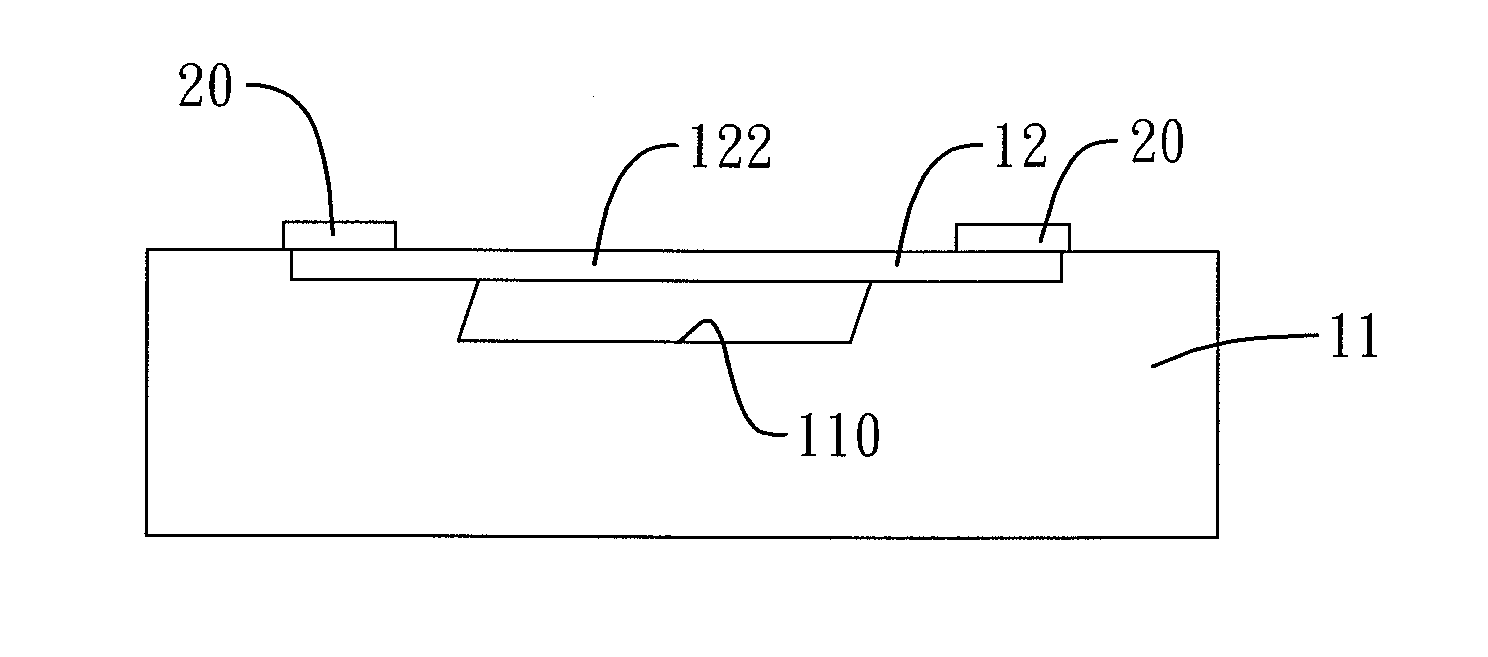
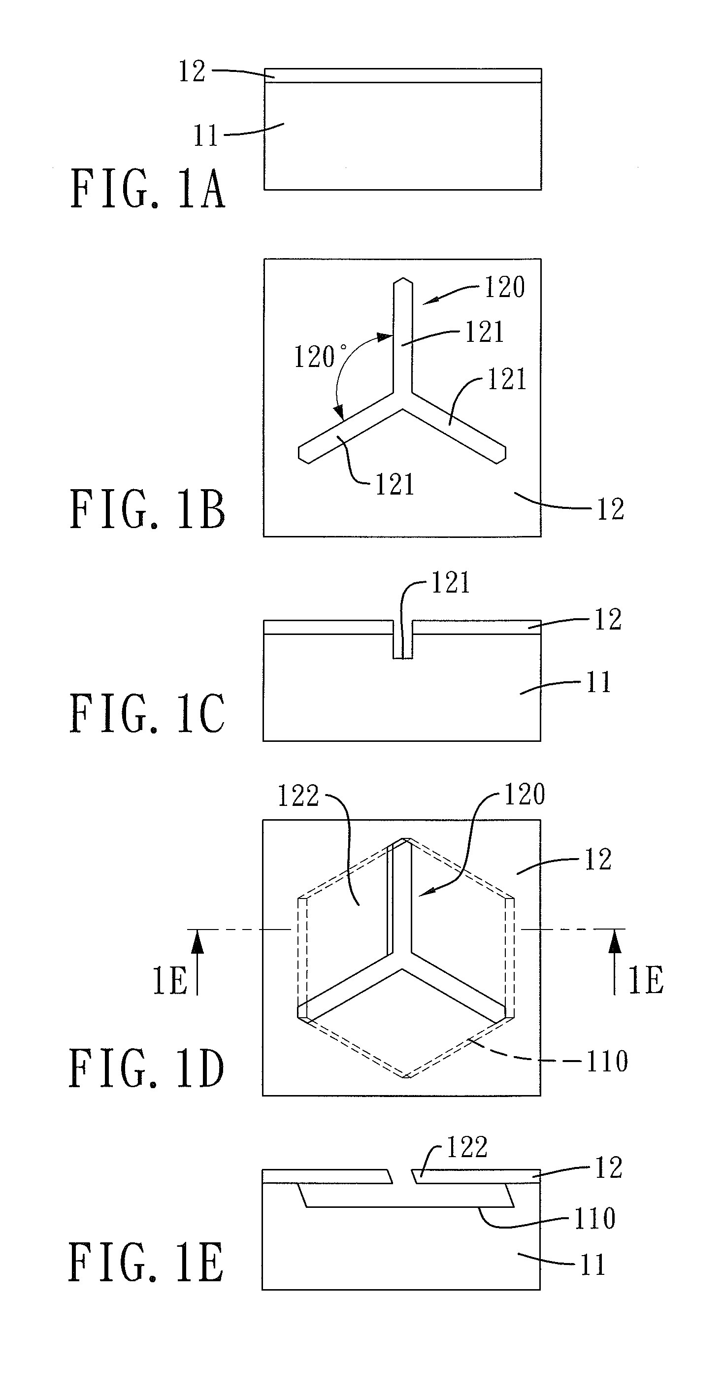
[0022]With reference to FIG. 1A, a single crystal silicon substrate 11 with a crystal orientation has a doped layer 12 formed on a top surface of the single crystal silicon substrate 11. In this embodiment, the doped layer 12 is formed on the top surface of the surface of the single crystal silicon substrate 11 by implanting impurity ions into the single crystal silicon substrate 11 or by a diffusion process, wherein the ions are selected from oxygen, boron or borofluoride. Impurity concentration of the doped layer 12 is higher than 1019cm3.

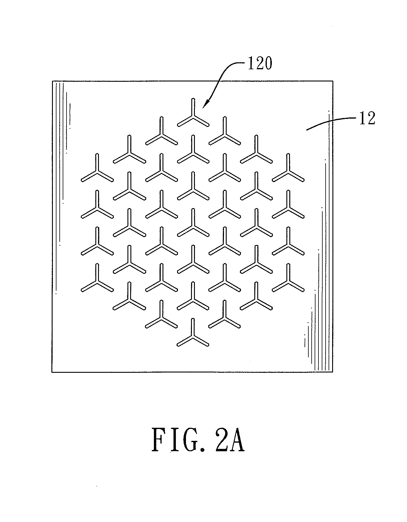
[0023]With reference to FIG. 1B and FIG. 1C, a main etching window 120 is formed through the doped layer 12. The main etching window 120 extends in parallel to a crystal plane {111}. The main etching window 120 could have three straight grooves 121. Each straight groove 121 has a depth more than the thickness of the doped layer 12. The depth of each straight groove 121 decides a depth of a cavity in the following steps.

[0024]Each of the straight...


PUM


Abstract

To form a single crystal silicon membrane with a suspension layer, a single crystal silicon substrate with crystal orientation <111> is prepared. A doped layer is formed on the top surface of the single crystal silicon substrate. Multiple main etching windows are formed through the doped layer. A cavity is formed through the single crystal silicon substrate by anisotropic etching. The doped layer is above the cavity to form a suspension layer. If two electrode layers are formed on the two ends of the suspension layer, a micro-heater is constructed. The main etching windows extend in parallel to a crystal plane {111}. By both the single crystal structure and different impurity concentrations of the single crystal silicon substrate, the single crystal silicon substrate has a higher etch selectivity. When a large-area cavity is formed, the thickness of the suspension layer is still controllable.

Description

BACKGROUND OF THE INVENTION[0001]1. Field of the Invention[0002]The present invention relates to a single crystal silicon membrane, and more particularity to a single crystal silicon membrane with a suspension layer, a method for fabricating the same and a micro-heater.[0003]2. Description of Related Art[0004]Forming a suspension layer in a silicon substrate may use a heavily doped etching stop technique. With reference to U.S. Pat. No. 5,116,457, a heavily doped layer is formed on a silicon substrate, and multiple etching windows are formed on the heavily doped layer. First, the silicon substrate is immersed into an anisotropic etching solution. The etch rate of the undoped silicon substrate in the anisotropic etching solution is much faster than that of heavily doped silicon layer, and the etch selectivity of undoped silicon to heavily doped silicon is typically around 50. By this characteristic, the anisotropic etching solution will remove a non-heavily doped silicon substrate re...

Claims


Application Information

Patent Timeline
Patent Type & Authority Applications(United States)
IPC IPC(8): H01L29/04H01L21/306
CPCB81C1/00158H05B3/141B81C2201/0136B81C1/00595
Inventor CHEN, CHUNG-NAN
Owner NAT KAOHSIUNG UNIV OF SCI & TECH
Why Eureka
Try Eureka