Surface plasmon resonance sensor and sensor chip

a surface plasmon resonance and sensor chip technology, applied in the direction of color/spectral property measurement, instruments, material analysis, etc., can solve the problems of large device size, high device cost, and difficult manufacturing of small s/n ratio and high sensitivity sensors

Active Publication Date: 2008-09-11
ORMON CORP
View PDF3 Cites 78 Cited by
  • Summary
  • Abstract
  • Description
  • Claims
  • Application Information

AI Technical Summary

Problems solved by technology

These become the cause of noise, and thus it becomes difficult to manufacture a sensor having small S / N ratio and high sensitivity.
In order to manufacture a sensor of high sensitivity, a step of removing foreign substances that become the cause of noise, and a strict temperature controlling means for maintaining the temperature of the test sample constant are required, whereby the device becomes larger and the device cost becomes expensive.
However, in sensors using surface plasmon resonance generated at the metal fine particles such as Au and Ag, the intensity of the signal obtained from the testing object attached to the surface of the metal fine particles is small, and thus the sensitivity is still low or the sensitivity is not sufficient in such regards.
Furthermore, the metal fine particles can be relatively easily separated if the distribution density of the metal fine particles is small, as shown in FIG. 6A, but the metal fine particles condense as shown within a circle in FIG. 6B if the distribution density of the metal fine particles becomes large, and it becomes difficult to stabilize the quality.
Therefore, a problem of mass production arises when commercializing, and in particular, mass productivity becomes worse when the distribution density of the metal fine particles is increased to enhance the sensitivity.
Therefore, about half a day is required to manufacture one sensor chip, and the manufacturing throughput is very low.
Therefore, mass production is difficult with such method, and realization of an inexpensive sensor chip is impossible.

Method used


Image

  • Surface plasmon resonance sensor and sensor chip
  • Surface plasmon resonance sensor and sensor chip
  • Surface plasmon resonance sensor and sensor chip

Examples


first embodiment

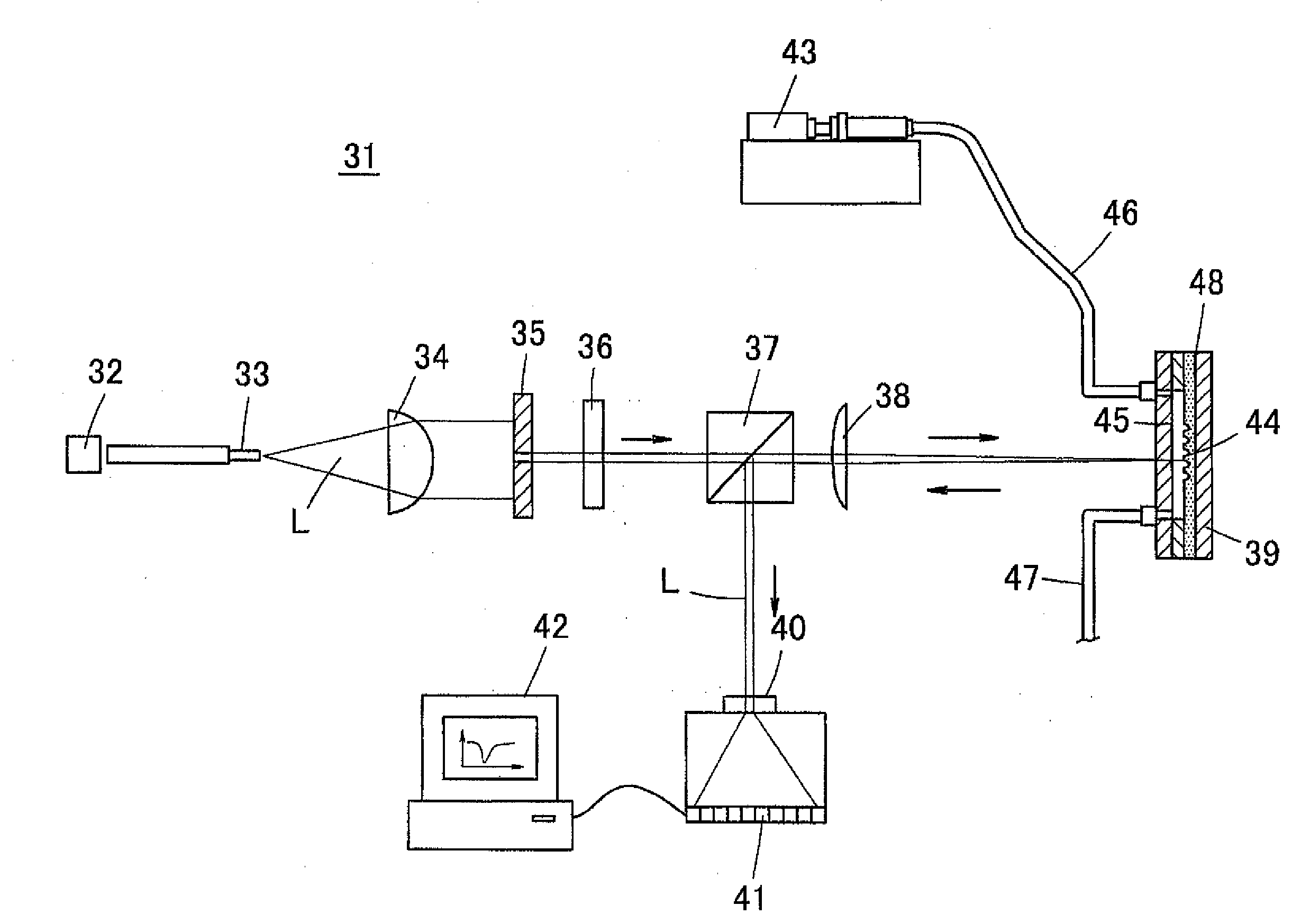
[0097]FIG. 9 shows a schematic view of a basic configuration of a local surface plasmon resonance sensor (hereinafter referred to as local SPR sensor) 31 according to a first embodiment of the present invention. The local SPR sensor 31 is configured by a light source 32 such as halogen lamp, an optical fiber 33, a collimator lens 34, a collimator plate 35 with pin holes, a polarization plate 36, a beam splitter 37 (or half mirror), an objective lens 38, a flow cell 48, a spectroscope 40, a photodetector 41, a data processing device 42, and a syringe pump 43.

[0098]The light source 32 is desirably that which irradiates a white light such as a halogen lamp, but may be of any type as long as it has light of a wavelength region used for measurement. Light L exit from the light source 32 is guided to the collimator lens 34 by the optical fiber 33. The collimator lens 34 collimates the light L exit from the distal end of the optical fiber 33, and passes the light as parallel beam. The ligh...

second embodiment

[0166]The sensor chip 39 according to a second embodiment of the present invention will be described. The sensor chip 39 of the second embodiment has a feature in that the central part of the bottom surface of the concave part 57 is raised towards the opening side.

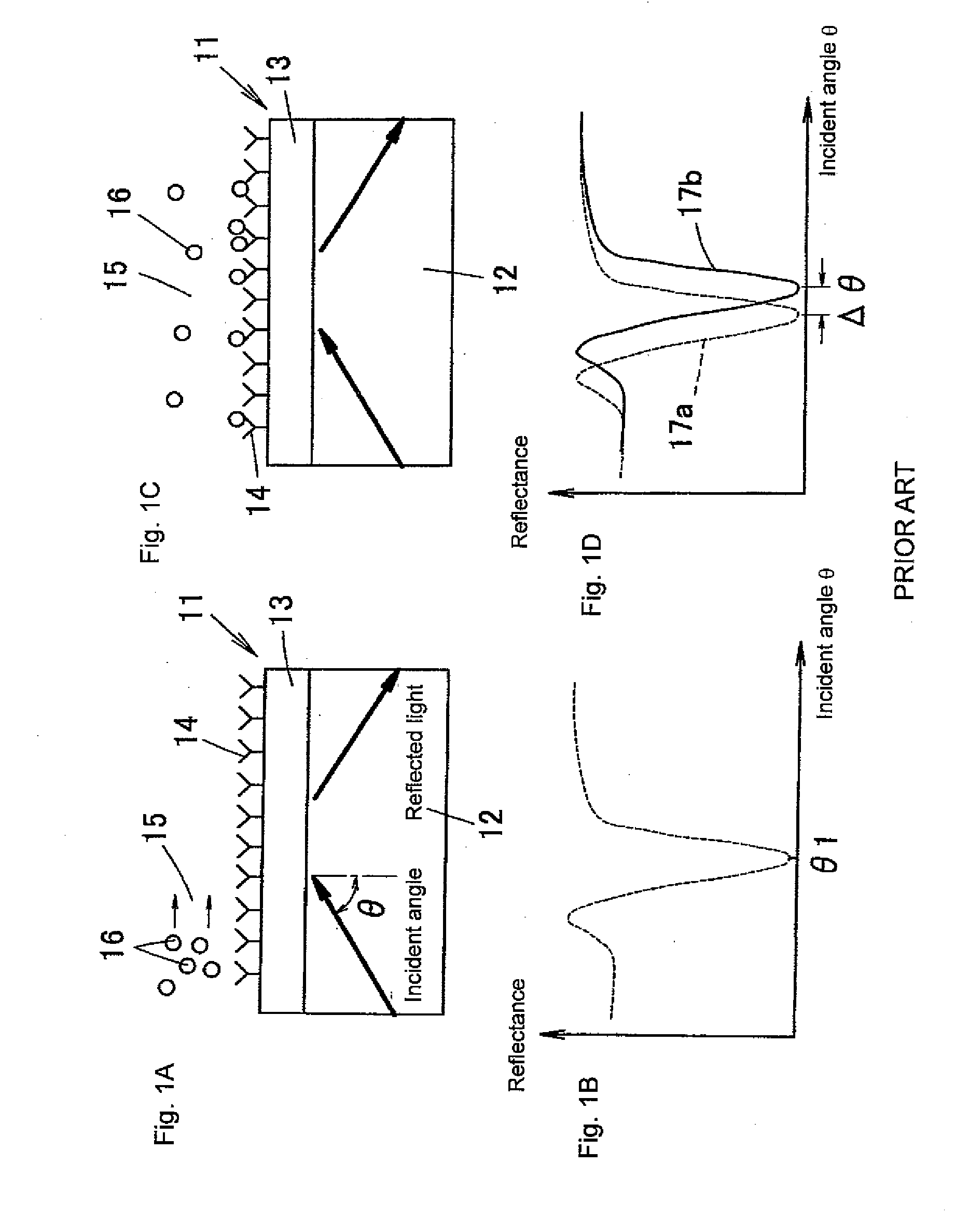
[0167]Looking at the electric field distribution generated inside the concave part 57 shown in FIG. 17 in detail, it can be seen that the electric field intensity is not as strong in the vicinity of the bottom part of the concave part 57. This is because the electric force line in the concave part 57 is raised to the opening side. Thus, when the bottom surface of the concave part 57 is a flat plane as in the first embodiment, even if a specific substance such as protein bonds to the bottom surface of the concave part 57 as shown in FIG. 32A, such specific substance is positioned in a region of small electric field intensity, and thus change in index of refraction by the specific substance does not greatly contribute to sig...

third embodiment

[0178]The concave structure of the sensor chip according to the second embodiment of the present invention will now be described. In the sensor chip of the third embodiment, the concave part 57 is divided into plurals in the longitudinal direction, as shown in FIG. 40, as opposed to the concave part 57 extending in a groove form from end to end of the measurement region 44 as in the first embodiment. Consequently, the concave part 57 has a substantially rectangular concave structure, and is lined along two directions orthogonal to each other.

[0179]The manner of arraying the concave part 57 may be rectangular array (manner of arraying in a grid form) or delta array (manner of arraying in a staggering manner as in FIG. 40B), and the case of delta array will be described herein. The concave part 57 is lined at a constant pitch P similar to the first embodiment in a direction parallel to the polarizing surface of the incident light, but the width S1 of the concave part 57 and width S2 o...


PUM

PropertyMeasurementUnit
widthaaaaaaaaaa
thicknessaaaaaaaaaa
inclination angleaaaaaaaaaa

Abstract

A sensor chip has a metal layer formed on a surface of a substrate, where a plurality of microscopic concave part is formed in a measurement region of the surface of the metal layer. When light of linear polarization is irradiated onto the measurement region, local resonance electric field generates at opposing metal layer surfaces in the concave part. The reflected light thereof is received to measure reflectance. The light of linear polarization is irradiated so that the polarizing surface becomes orthogonal to the longitudinal direction of the concave part.

Description

BACKGROUND OF THE INVENTION[0001]1. Technical Field[0002]The present invention relates to a surface plasmon resonance sensor and a sensor chip. In particular, the present invention relates to a surface plasmon resonance sensor that uses a local surface plasmon resonance, and a surface plasmon resonance sensor chip.[0003]2. Related Art[0004]Human body consists of 60% water, and 40% of the remaining half protein, where the majority of the tissues, muscles, and skin of the human body consist of protein. Thus, a correlation is often recognized between the disease and the variation of the protein, where a specific protein increases in the body (e.g., in the blood) with progression of the disease in cancer, influenza, and other diseases.[0005]Therefore, the affected site and the progressing state of the disease can be recognized by monitoring the state of a specific protein (presence, amount, etc. of a specific protein), and currently, a correlation with the disease is recognized for a fe...

Claims


Application Information

Patent Timeline
Patent Type & Authority Applications(United States)
IPC IPC(8): G01N21/55B82Y15/00G01N21/27G01N21/41
CPCB82Y15/00G01N21/05G01N2021/0346G01N2021/054G01N21/554G01N21/253G01N2021/0378G01N2021/0382
Inventor NISHIKAWA, TAKEOMATSUSHITA, TOMOHIKOYAMASHITA, HIDEYUKIHASUI, RYOSUKEFUJITA, SATOSHIOKUNO, YUTAROAOYAMA, SHIGERU
Owner ORMON CORP
Why Eureka
Try Eureka