MOS transistor triggered transient voltage supressor to provide circuit protection at a lower voltage

a transient voltage and suppressor technology, applied in the direction of circuit arrangements, electrical equipment, and electrical devices responsive to excess voltage, can solve the problems of large area to reduce resistance, circuit damage, unexpected and uncontrollable high voltage hitting the circuit, etc., to achieve the effect of reducing voltage and improving clamping

Active Publication Date: 2008-09-11
ALPHA & OMEGA SEMICON LTD
View PDF18 Cites 52 Cited by
  • Summary
  • Abstract
  • Description
  • Claims
  • Application Information

AI Technical Summary

Benefits of technology

[0010]Another aspect of this invention is to provide TVS protection circuit with tunable low trigger voltage between 3.3 to 5 volts with low leakage implemented by stacking PMOS diodes.
[0012]Another aspect of this invention is to provide TVS protection circuit with a tunable low trigger voltage between 3.3 to 5 volts by implementing the TVS protection circuit with the high side diodes with NBL to suppress the I / O-to-I / O latch-up such that the device performance is further improved.

Problems solved by technology

However, in situations such as electrostatic discharge (ESD), electrical fast transients and lightning, an unexpected and an uncontrollable high voltage may accidentally strike onto the circuit.
Since the Zener diode has higher resistance per unit area compared with BJT or SCR and BJT this is actually a disadvantage at higher currents because the steering diodes also have to be rugged in reverse conduction.
The problem with the Vcc-Gnd clamp diodes is that typically these diodes are very resistive in reverse blocking mode and require large area to reduce resistance.
This is not desirable as high BV not only causes the break down of steering diodes as described above but also causes damage to the circuit the TVS device intends to protect.
The requirement to have large diode size thus limits further miniaturization of a device when such TVS circuit is implemented.
However, in a device that implements a TVS circuit, the snap-back phenomenon is not desirable.
The snap-back creates a sudden drop of the reverse voltage that often causes the circuit oscillations due to negative resistance.
However, in addition to the technical difficulties related to the sudden large voltage drops as discussed above, there is a need to reduce the transient voltage protection at a further reduced voltage such as 3.3 volts.
The TVS circuits disclosed have been effective to protective circuit operated at about five volts, however, would not provide the required protection when the operational voltage is further reduced below five volts as the increasing leakage current of trigger diode would make it practically inoperable.

Method used


Image

  • MOS transistor triggered transient voltage supressor to provide circuit protection at a lower voltage
  • MOS transistor triggered transient voltage supressor to provide circuit protection at a lower voltage
  • MOS transistor triggered transient voltage supressor to provide circuit protection at a lower voltage

Examples


Embodiment Construction

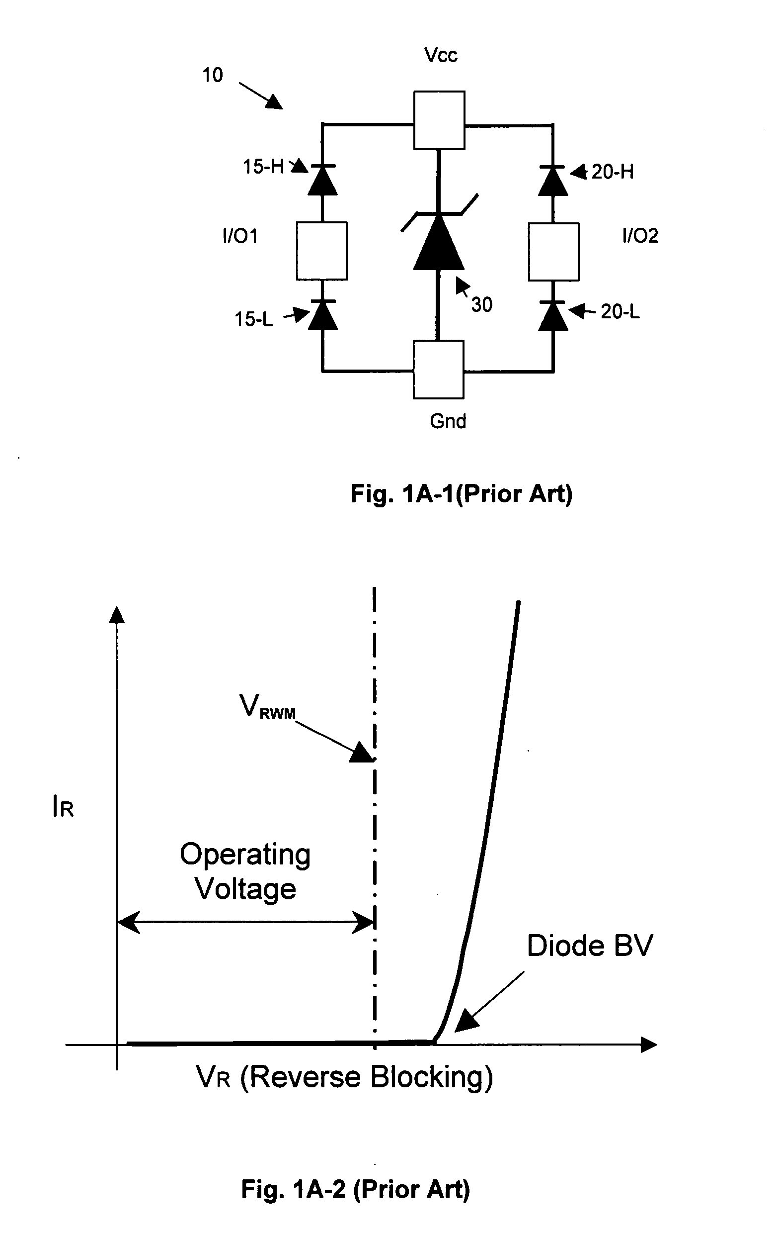
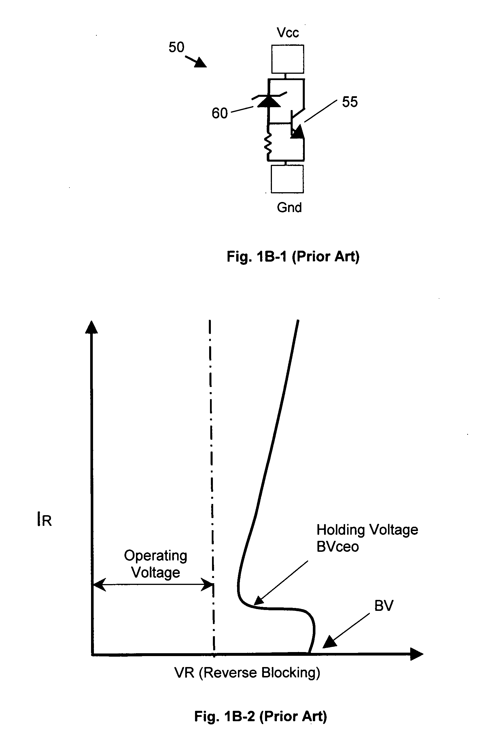
[0025]For better understanding of this invention, the descriptions of the FIGS. 2A and 2B below are provided as background reference information of the TVS disclosed previously by a common invention of this application. FIGS. 2A and 2B are respectively a circuit diagram and an I-V diagram, i.e., a current versus voltage diagram, of a TVS circuit 100 disclosed in application Ser. No. 11 / 444,555. The TVS circuit 100 is installed between a ground voltage terminal (Gnd) 105 and a Vcc voltage terminal 110 to function as a Vcc-Gnd clamp circuit. The TVS circuit 100 includes two sets of steering diodes, i.e., diodes 115-H and 115-L and 120-H and 120-L respectively for each of the two input / output (I / Os) terminals 125-1 and 125-2. Furthermore, there is a Zener diode, i.e., diode 130, with a larger size to function as an avalanche diode from the high voltage terminal, i.e., terminal Vcc, to the ground voltage terminal, i.e., terminal Gnd. The Zener diode 130 is connected in series with a res...


PUM

PropertyMeasurementUnit
transient voltageaaaaaaaaaa
voltageaaaaaaaaaa
voltageaaaaaaaaaa

Abstract

An electronic device formed as an integrated circuit (IC) wherein the electronic device further includes a transient voltage suppressing (TVS) circuit. The TVS circuit includes a triggering MOS transistor connected between an emitter and a collector of a first bipolar-junction transistor (BJT) coupled to a second BJT to form a SCR functioning as a main clamp circuit of the TVS circuit. The TVS circuit further includes a triggering circuit for generating a triggering signal for the triggering MOS transistor wherein the triggering circuit includes multiple stacked MOS transistors for turning into a conductive state by a transient voltage while maintaining a low leakage current.

Description

BACKGROUND OF THE INVENTION[0001]1. Field of the Invention[0002]The invention relates generally to a circuit configuration and method of manufacture of a transient voltage suppressor (TVS). More particularly, this invention relates to an improved circuit configuration and method of manufacture of a transient voltage suppressor (TVS) triggered by a MOS thus providing a voltage suppression protection at a significantly reduced voltage, e.g., at 3.3 volts.[0003]2. Description of the Relevant Art[0004]The transient voltage suppressors (TVS) are commonly applied for protecting integrated circuits from damages due to the inadvertent occurrence of an over voltage imposed onto the integrated circuit. An integrated circuit is designed to operate over a normal range of voltages. However, in situations such as electrostatic discharge (ESD), electrical fast transients and lightning, an unexpected and an uncontrollable high voltage may accidentally strike onto the circuit. The TVS devices are re...

Claims


Application Information

Patent Timeline
Patent Type & Authority Applications(United States)
IPC IPC(8): H02H3/20
CPCY10T29/49002H01L27/0262
Inventor MALLIKARARJUNASWAMY, SHEKARBOBDE, MADHUR
Owner ALPHA & OMEGA SEMICON LTD
Why Eureka
Try Eureka