Method for manufacturing organic electroluminescence panel

a technology of electroluminescence panel and manufacturing method, which is applied in the direction of paper/cardboard containers, transportation and packaging, containers, etc., can solve the problems of cracking or peeling of protective layers, complicating the manufacturing process, and the step of removing masks, so as to simplify the manufacturing process

Active Publication Date: 2008-09-11
CANON KK
View PDF5 Cites 27 Cited by
  • Summary
  • Abstract
  • Description
  • Claims
  • Application Information

AI Technical Summary

Benefits of technology

[0010]Accordingly, the present invention solves the problem that cutting or severing a protective layer may cause cracking or peeling of the protective layer, as in the Japanese Patent Laid-Open No. 2003-249354, and simplifies the manufacturing process, which is difficult to achieve in the Japanese Patent Laid-Open No. 2003-249354.
[0013]According to the present invention, the substrate and the protective layer are cut from the substrate side while the laminate member is in contact with the protective layer. The laminate member therefore prevents cracking or peeling of the protective layer during the process of cutting the protective layer. In addition, cutting both the substrate and the protective layer in a single step can simplify the manufacturing process. Thus, the present invention produces an organic electroluminescence panel that includes a protective layer substantially free from cracking or peeling by a simple method.

Problems solved by technology

During this severing procedure cracking or peeling of the protective layer may occur.
In addition, the step of removing the mask after the formation of the protective layer complicates the manufacturing process.

Method used


Image

  • Method for manufacturing organic electroluminescence panel
  • Method for manufacturing organic electroluminescence panel
  • Method for manufacturing organic electroluminescence panel

Examples


example 1

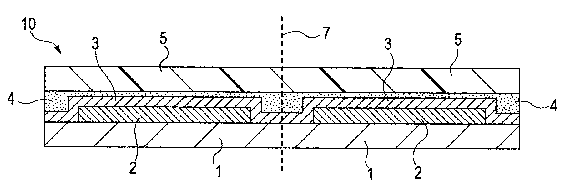
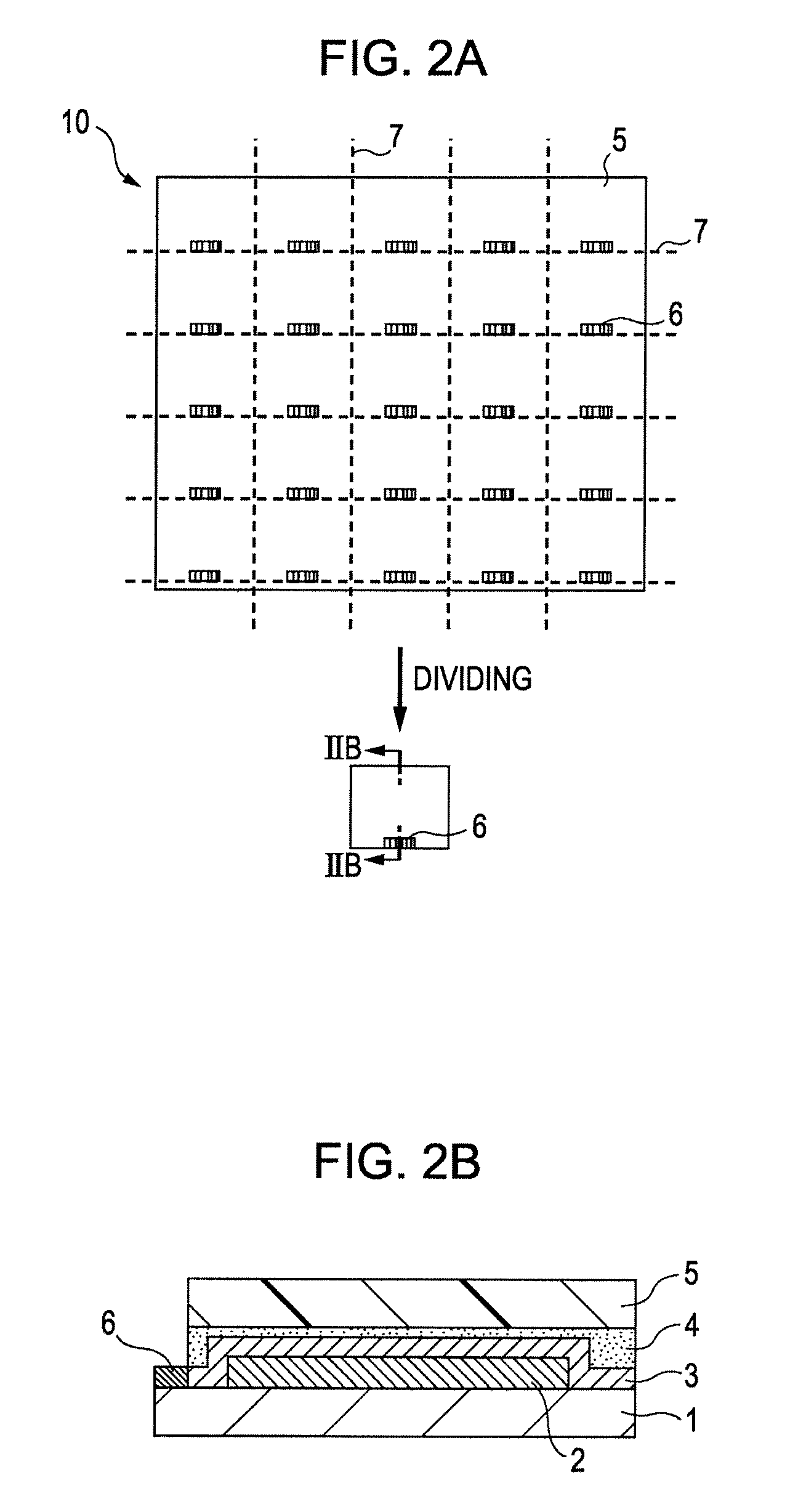
[0040]An embodiment according to the present invention will be described below with reference to FIG. 3.

[Planarizing Film]

[0041]An acrylic planarizing film was formed by photolithography on a glass substrate, on which TFT circuits of a plurality of panels were disposed, to flatten recessed and raised portions due to the TFT circuits.

[Formation of Chromium Electrode]

[0042]A chromium film having a thickness of 100 nm was deposited as an anode on the planarizing film by direct-current sputtering of a chromium target. The chromium film was formed as a pixel electrode 20 μm×100 μm in size using photolithography. The sputtering was performed in an atmosphere of argon at a pressure of 0.2 Pa and an electric power of 300 W.

[Open to the Atmosphere]

[0043]The specimen was removed from the sputtering apparatus, was subjected to ultrasonic cleaning in acetone and then isopropyl alcohol (IPA), was washed in boiling IPA, was dried, and was subjected to UV / ozone cleaning.

[Device Isolation Film]

[004...


PUM


Abstract

A substrate, an array of organic electroluminescence element groups disposed on the substrate, each organic electroluminescence element group formed of a plurality of organic electroluminescence elements, a protective layer disposed on the array of organic electroluminescence element groups, and a laminate member disposed on the protective layer were divided between the array of organic electroluminescence element groups into a plurality of organic electroluminescence panels.

Description

BACKGROUND OF THE INVENTION[0001]1. Field of the Invention[0002]The present invention relates to a method for manufacturing an organic electroluminescence panel.[0003]2. Description of the Related Art[0004]One of known organic electroluminescence panels has an organic electroluminescence element that is disposed on a glass substrate and that has a sandwich structure in which an organic luminescent layer is sandwiched between two electrodes. One of the two electrodes is a transparent electrode, in general, formed of indium tin oxide (ITO), to extract light from the organic luminescent layer. The outer surface of the organic luminescent layer is sealed. The organic luminescent layer emits light upon the application of a voltage by an external drive circuit.[0005]Organic electroluminescence panels that include an organic electroluminescence element that emits light according to the above-mentioned principle have excellent legibility and produce various colors. Hence, the organic electr...

Claims


Application Information

Patent Timeline
Patent Type & Authority Applications(United States)
IPC IPC(8): B05D5/12
CPCH01L51/56H01L2251/566Y10T156/1057Y10T156/10H01L51/5237Y10T156/1056Y10T156/1052H10K50/8426H10K50/844H10K71/851H10K71/00
Inventor KATAOKA, ICHIRO
Owner CANON KK
Why Eureka
Try Eureka