

Method of producing n-type group-13 nitride semiconductor, method of forming current confinement layer, method of producing surface emitting laser, method of changing resistance of nitride semiconductor and method of producing semiconductor laser
a technology of nitride semiconductor and current confinement layer, which is applied in the direction of semiconductor lasers, lasers, electrical equipment, etc., can solve the problems of affecting the quality of crystals before and after regrowth, poor electrical properties, and volume change, and achieve the effect of increasing resistan
- Summary
- Abstract
- Description
- Claims
- Application Information
AI Technical Summary
Benefits of technology
Problems solved by technology
Method used
Image

Examples
example 1
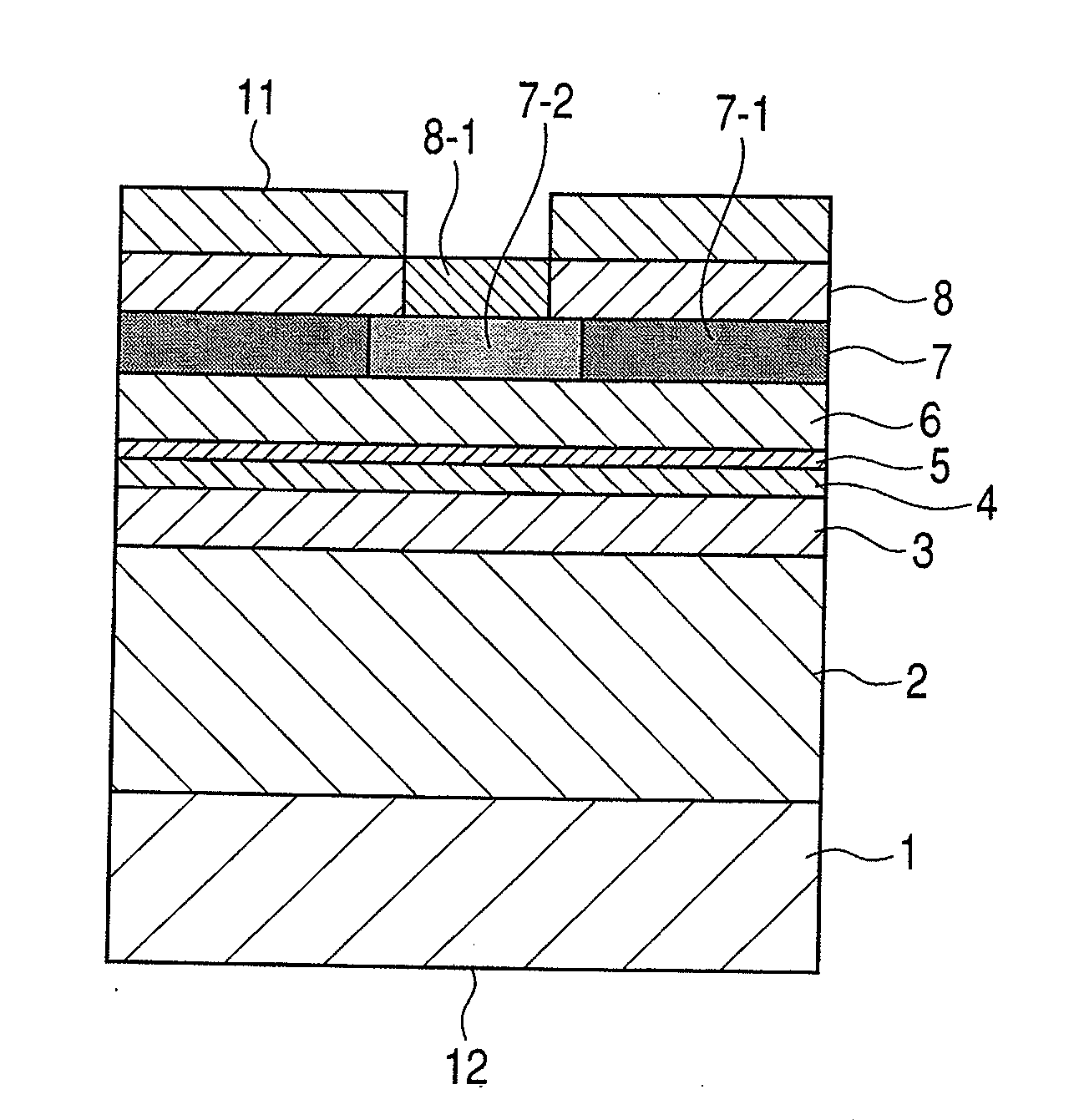
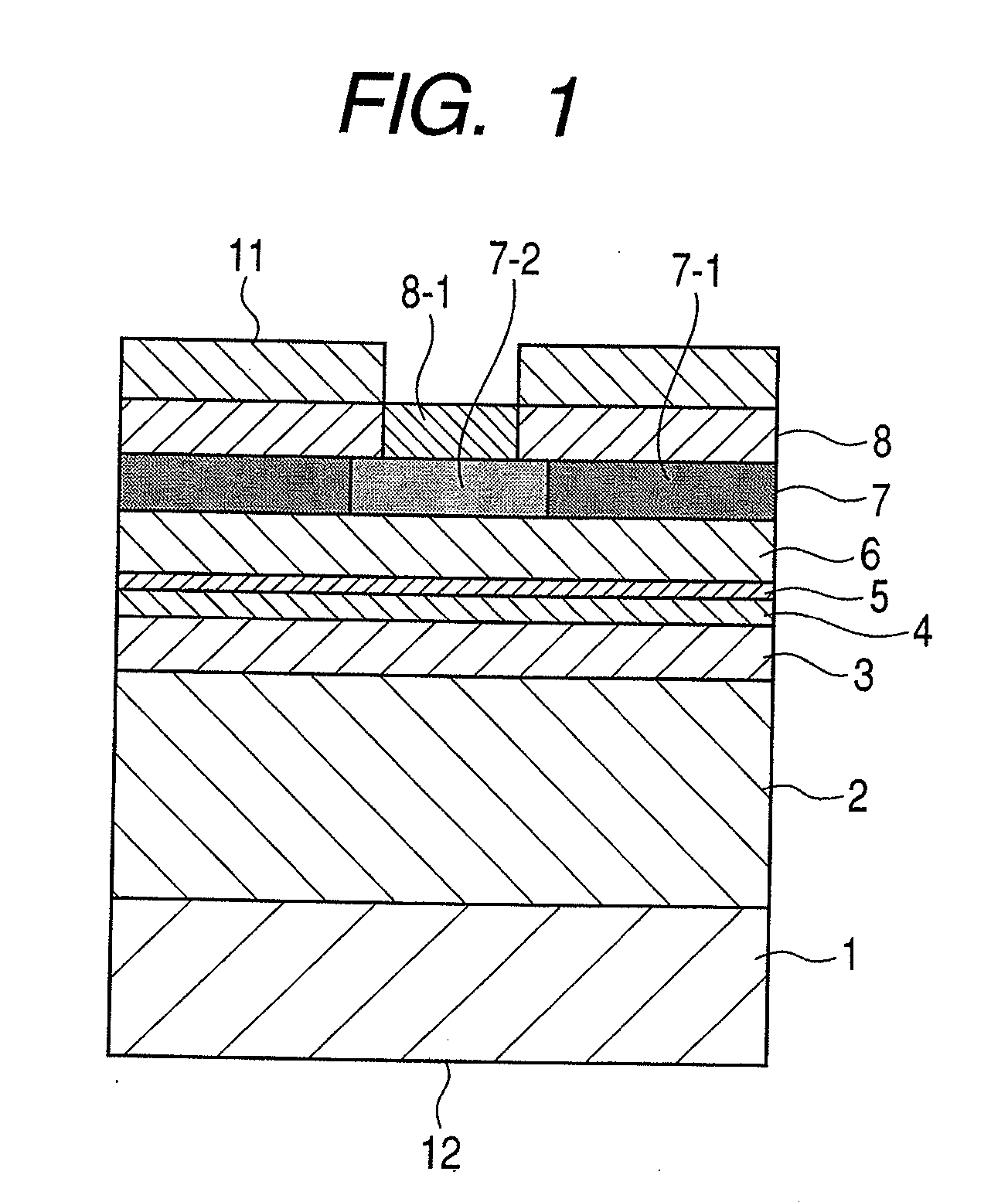
[0100]n-Type gallium nitride substrates of 2 inches in size were obtained from several manufacturers and subjected to epitaxial growth using the composition ratios shown in Table 1.
[0101]The thickness obtained by epitaxial growth was optimized by oscillation wavelength. The Layer 14 and the Absorb layer, which are the characteristics of the present invention, were grown to 100 nm and 400 nm, respectively.
[0102]A light shield mask was formed on a region, which is to be a current confinement layer opening, of the surface of the n-type AlGaN contact layer, shown by Layer 14, and the Layer 14 was irradiated with light of YAG THG laser as a laser for material processing. Beam profile was shaped into a flattop profile by an optical system under the laser conditions of wavelength: 355 nm, pulse width: 5 nanoseconds, repeat frequency: 10 Hz, and energy density: 50 mJ / cm2. The monochromaticity of YAG THG laser light is high and controlled to be within the range of ±0.1 nm.
[0103]For the n-typ...
example 2
[0110]A semiconductor laser was produced under the same conditions as in Example 1 except that an XeF excimer laser was used as a laser for material processing.
[0111]The laser conditions were as follows: wavelength 351±0.1 nm, pulse width 20 nanoseconds, repeat frequency 10 Hz, energy density 40 mJ / cm2.
example 3
[0112]A semiconductor laser was produced under the same conditions as in Example 1 except that a nitrogen laser was used as a laser for material processing and an n-type Al0.2Ga0.8N (Eg=3.79 eV=327 nm) was used for the contact layer.
[0113]The laser conditions were as follows: wavelength 337±0.1 nm, pulse width 4 nanoseconds, repeat frequency 10 Hz, energy density 20 mJ / cm2.
PUM
| Property | Measurement | Unit |
|---|---|---|
| thickness | aaaaa | aaaaa |
| wavelength | aaaaa | aaaaa |
| resistivity | aaaaa | aaaaa |
Abstract
Description
Claims
Application Information