Cascode current mirror and method

a current mirror and cascode technology, applied in the field of semiconductor devices for fabricating semiconductor devices, can solve the problems of current mirror matching between the devices that make up reference and current mirror, noise performance worsening, and the trend of reducing supply voltag

Active Publication Date: 2008-09-18
NXP USA INC
View PDF2 Cites 19 Cited by
  • Summary
  • Abstract
  • Description
  • Claims
  • Application Information

AI Technical Summary

Benefits of technology

[0044]According to a first embodiment, there is provided a cascode current mirror device, comprising, first and second series coupled MOS transistors adapted to form a reference current path of the current mirror device, wherein the first and second transistors have first and second gates overlying first and second gate dielectrics of first and second thicknesses, respectively, and the first and second transistors have first and second channel lengths and channel widths, respectively, and each transistor has a source and a drain and the source of the first transistor forms a first node, the drain of the first transistor is coupled to the source of the second transistor at a second node and the drain of the second transistor forms a third node, and wherein the current mirror device is adapted to have a reference current flow between the first and third nodes, and third and fourth series coupled MOS transistors adapted to form a mirror current path of the current mirror device, wherein the third and fourth transistors have third and fourth gates overlying third and fourth gate dielectrics of third and fourth thicknesses, respectively, and the third and fourth transistors have third and fourth channel lengths and channel widths, respectively, and each transistor has a source and a drain, and the source of the third transistor forms a fourth node, the drain of the third transistor is coupled to the source of the fourth transistor and the drain of the fourth transistor forms a fifth node, and the first and third gates are coupled together and to the second node and the second and fourth gates are coupled together and to the third node, and wherein the mirror current devices is adapted to have a mirror current flow between the fourth and fifth nodes, and wherein gate dielectric thicknesses of the first and third transistors are smaller than gate dielectric thicknesses of the second and fourth transistors, and wherein channel lengths of the first and third transistors are larger than channel lengths of the second and fourth transistors. According to a further embodiment, the first or third transistors have a ratio RBnew of channel length to channel width in a range of about 1.5≦RBnew≦20. According to a still further embodiment, the first or third transistors have a ratio RBnew of channel length to channel width in a range of about 2≦RBnew≦10. According to a yet further embodiment, the first or third transistors have a ratio RBnew of channel length to channel width in a range of about 2≦RBnew≦4. According to a still yet further embodiment, the first gate dielectric thickness of the first transistor is in a range of about 10 to 90 percent of the second gate dielectric thickness of the second transistor. According to a yet still further embodiment, the first gate dielectric thickness of the first transistor is in a range of about 20 to 50 percent of the second gate dielectric thickness of the second transistor. According to an additional embodiment, the first gate dielectric thickness of the first transistor is in a range of about 30 to 40 percent of the second gate dielectric thickness of the second transistor. According to a still additional embodiment, the second or fourth transistors have a ratio RTnew of channel length to channel width in a range of about 0.2≦RTnew≦1. According to a yet additional embodiment, the second or fourth transistors have a ratio RTnew of channel length to channel width in a range of about 0.4≦RTnew≦1.

Problems solved by technology

However, as the devices making up the cascode mirror are reduced in size, the matching between the devices that make up reference and current mirror sides 401, 402 deteriorates and the noise performance worsens.
A further problem is that there is an ongoing trend to reduce supply voltages.
This means that the voltage available to provide gate overdrive voltage is also decreasing.
For the same threshold voltage Vth, if the available supply voltage Vsupp is reduced, the available overdrive voltage Vod is also reduced and the worse the mismatch and noise problems become.
Thus, as supply voltages are reduced, mismatch and noise problems become more severe.
While the increased mismatch and noise associated with lower operating voltages can be avoided or mitigated by increasing the gate area, this is not an economically viable solution for advanced smaller area circuits.

Method used


Image

  • Cascode current mirror and method
  • Cascode current mirror and method
  • Cascode current mirror and method

Examples


first embodiment

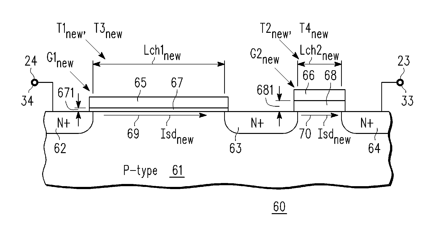
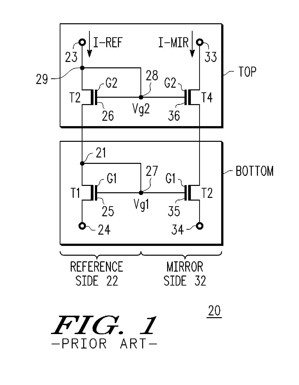
[0044] there is provided a cascode current mirror device, comprising, first and second series coupled MOS transistors adapted to form a reference current path of the current mirror device, wherein the first and second transistors have first and second gates overlying first and second gate dielectrics of first and second thicknesses, respectively, and the first and second transistors have first and second channel lengths and channel widths, respectively, and each transistor has a source and a drain and the source of the first transistor forms a first node, the drain of the first transistor is coupled to the source of the second transistor at a second node and the drain of the second transistor forms a third node, and wherein the current mirror device is adapted to have a reference current flow between the first and third nodes, and third and fourth series coupled MOS transistors adapted to form a mirror current path of the current mirror device, wherein the third and fourth transisto...

second embodiment

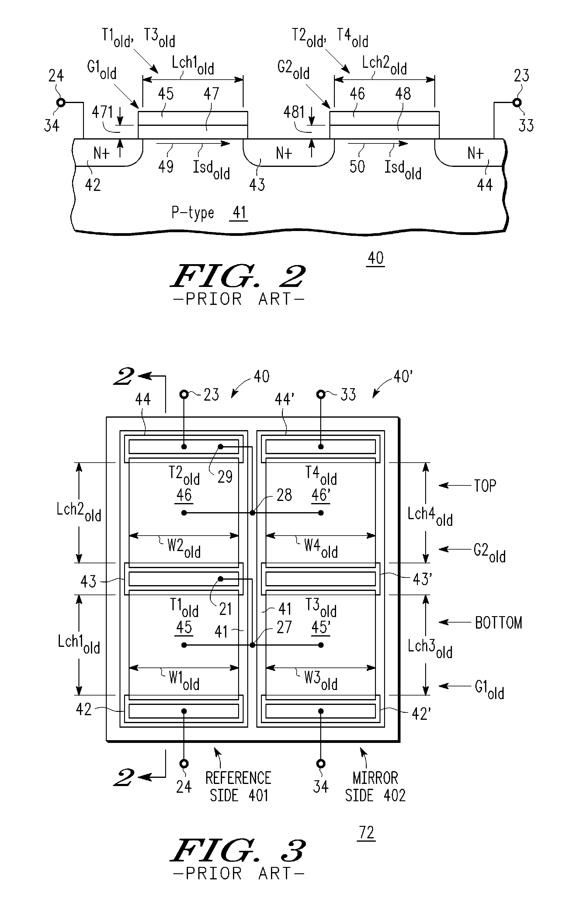
[0045] there is provided a method for forming a cascode current mirror using MOS transistors, comprising, providing a semiconductor substrate of a first conductivity type, and forming a first dielectric layer on a first portion of the semiconductor substrate, and forming a second dielectric layer on a second, different, portion of the semiconductor substrate and thinner than the first dielectric layer and forming a conductor over the first and second dielectric layers, and forming from the conductor, first and third spaced apart gates on the second dielectric layer over the second portion of the semiconductor substrate and second and fourth spaced apart gates on the first dielectric layer over the first portion of the semiconductor substrate, and doping multiple spaced apart regions of the substrate with a dopant of a second, opposite conductivity type, thereby forming source and drain regions in the substrate, wherein a first source regions is adjacent a first lateral side of the f...

third embodiment

[0046] there is provided a cascode current mirror, comprising, first and second series coupled MOSFETs, each MOSFET having source, drain, gate and gate dielectric, wherein the drain of the first MOSFET is coupled to the source of the second MOSFET and the first and second series coupled MOSFETS are adapted to provide a reference current path between a source of the first MOSFET and a drain of the second MOSFET, and third and fourth series coupled MOSFETs, each MOSFET having source, drain, gate and gate dielectric, wherein the drain of the third MOSFET is coupled to the source of the fourth MOSFET and the third and fourth series coupled MOSFETS are adapted to provide a mirror current path between a source of the third MOSFET and a drain of the fourth MOSFET, and wherein gates of the first and third MOSFETs are coupled together and to the drain of the first MOSFET and gates of the second and fourth MOSFETs are coupled together and to the drain of the second MOSFET, and wherein the gat...


PUM


Abstract

A cascode amplifier (CA) (60) is described having a bottom transistor (T1new) with a relatively thin gate dielectric (67) and higher ratio (RB) of channel length (Lch1new) to width (W1new) and a series coupled top transistor (T2new) with a relatively thick gate dielectric (68) and a lower ratio (RT) of channel length (Lch2new) to width (W2new). An improved cascode current mirror (CCM) (74) is formed using a coupled pair of CAs (60, 60′), one (60) forming the reference current (RC) side (601) and the other (60′) forming the mirror current side (602) of the CCM (74). The gates (65, 65′) of the bottom transistors (T1new, T3new) are tied together and to the common node (21) between the series coupled bottom (T1new) and top (T2new) transistors of the RC side (601), and the gates (66′, 66′) of the top transistors (T2new, T4new) are coupled together and to the top drain node (64) of the RC side (601). The area of the CCM (74) can be substantially shrunk without adverse affect on the matching, noise performance and maximum allowable operating voltage.

Description

FIELD OF THE INVENTION[0001]The present invention generally relates to semiconductor devices and methods for fabricating semiconductor devices, and more particularly relates to cascode current mirrors and methods therefore.BACKGROUND OF THE INVENTION[0002]Processing technologies and device structures for forming integrated circuits (ICs) are often implemented by using a plurality of interconnected field effect transistors (FETs), also called metal-oxide-semiconductor field effect transistors (MOSFETs), or simply MOS transistors or devices. Although the term “MOS” properly refers to a device having a metal gate electrode and an oxide gate insulator, that term will be used throughout to refer to any semiconductor device that includes a conductive gate electrode (whether metal or not) that is positioned over a gate insulator (whether oxide or other dielectric material) which, in turn, is positioned over a semiconductor surface. Accordingly, the terms metal-oxide-semiconductor and the a...

Claims


Application Information

Patent Timeline
Patent Type & Authority Applications(United States)
IPC IPC(8): H01L29/76
CPCH01L21/823425H01L21/823456H01L29/7833H01L27/088H01L29/6659H01L21/823462Y10S438/981
Inventor YANG, HONGNINGPERKINS, GEOFFREY W.ZUO, JIANG-KAI
Owner NXP USA INC
Why Eureka
Try Eureka