

Semiconductor device
a semiconductor and device technology, applied in the field of semiconductor devices, can solve the problems of high process cost in manufacturing semiconductor devices from compound semiconductors, difficulty in increasing the wafer diameter, and high material cost of compound semiconductors, and achieve the problem of increasing the harmonics, especially second harmonics, of rf signals in devices including radio frequency circuits on silicon substrates
- Summary
- Abstract
- Description
- Claims
- Application Information
AI Technical Summary
Benefits of technology
Problems solved by technology
Method used
Image

Examples
first embodiment
[0033]First, the invention is described.
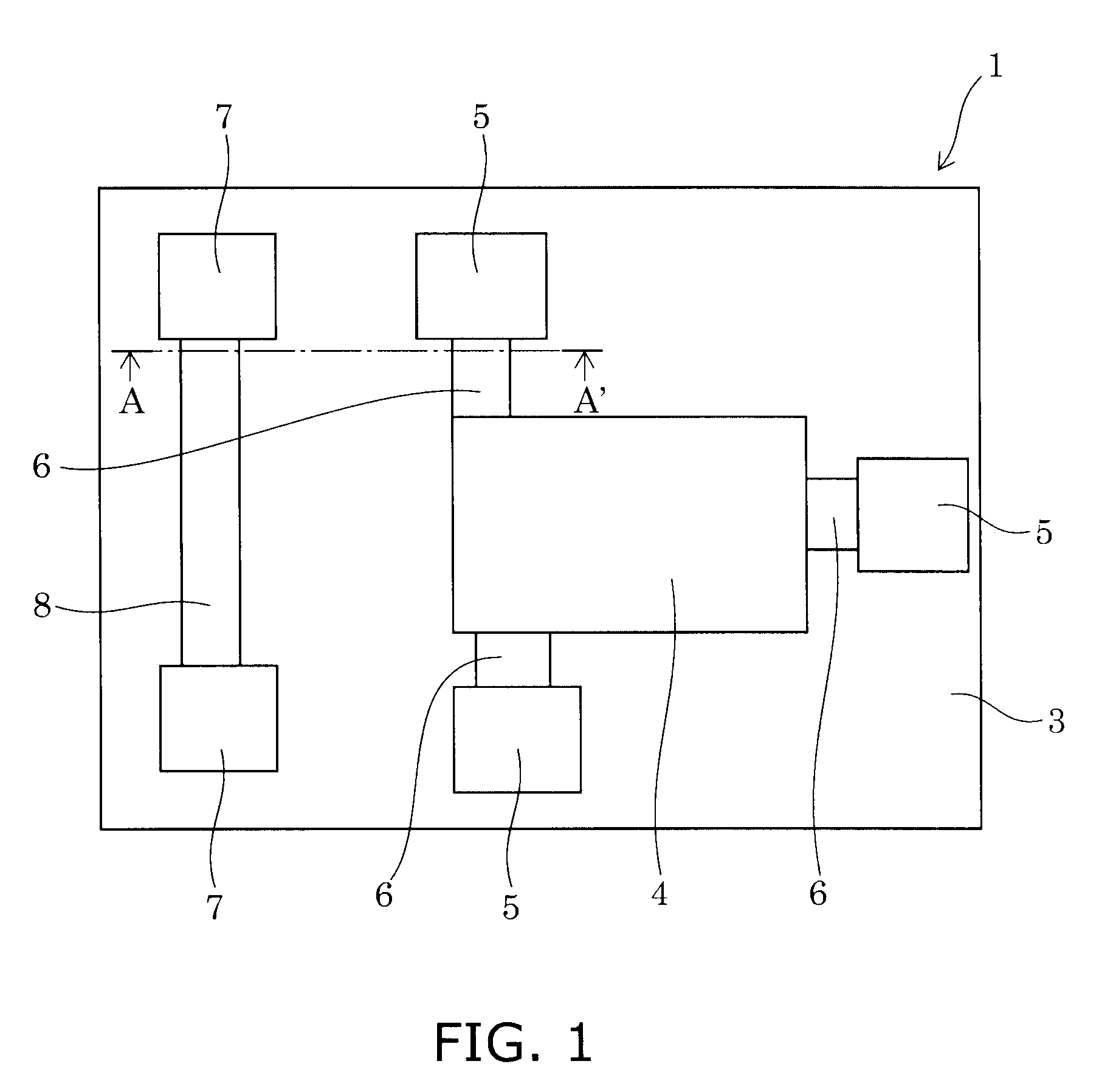
[0034]FIG. 1 is a plan view illustrating a semiconductor device according to this embodiment.
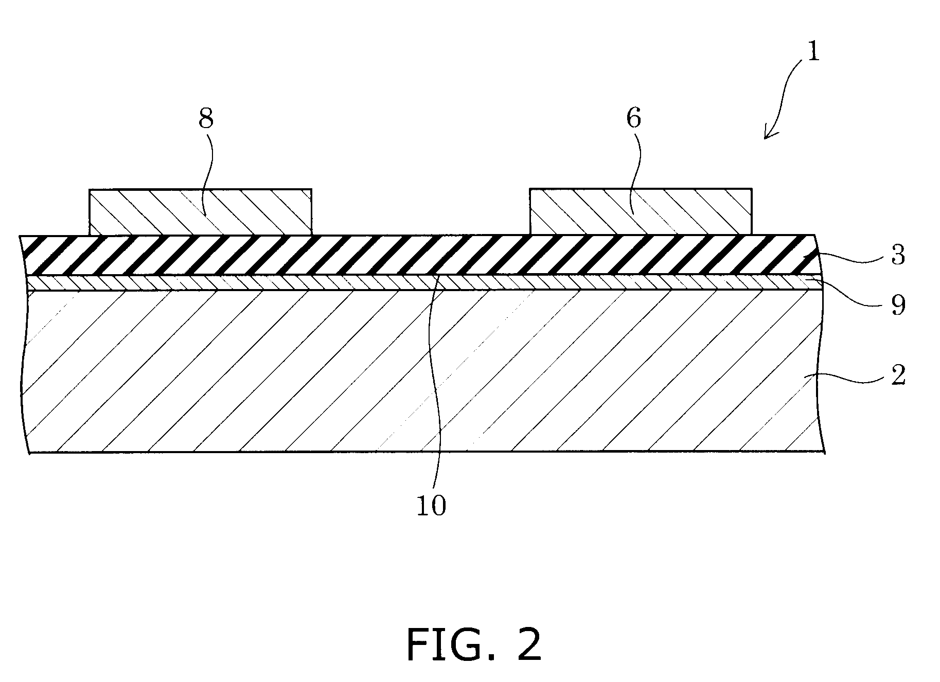
[0035]FIG. 2 is a cross-sectional view taken along line A-A′ shown in FIG. 1.
[0036]FIG. 3 is a graph illustrating a boron concentration profile in the silicon substrate along the depth, where the horizontal axis represents distance from the interface between the silicon substrate and the silicon oxide film, and the vertical axis represents boron concentration.
[0037]As shown in FIGS. 1 and 2, the semiconductor device 1 according to this embodiment receives as input a radio frequency signal (RF signal) having a frequency of 500 MHz or more and a power of 20 dBm (=100 mW) or more. For example, in a mobile communication apparatus, the semiconductor device 1 serves as a radio frequency switch circuit through which an antenna is connected to a transmitting circuit and a receiving circuit.
[0038]The semiconductor device 1 includes a silicon substrate 2 made of...
second embodiment
[0063]Next, the invention is described.
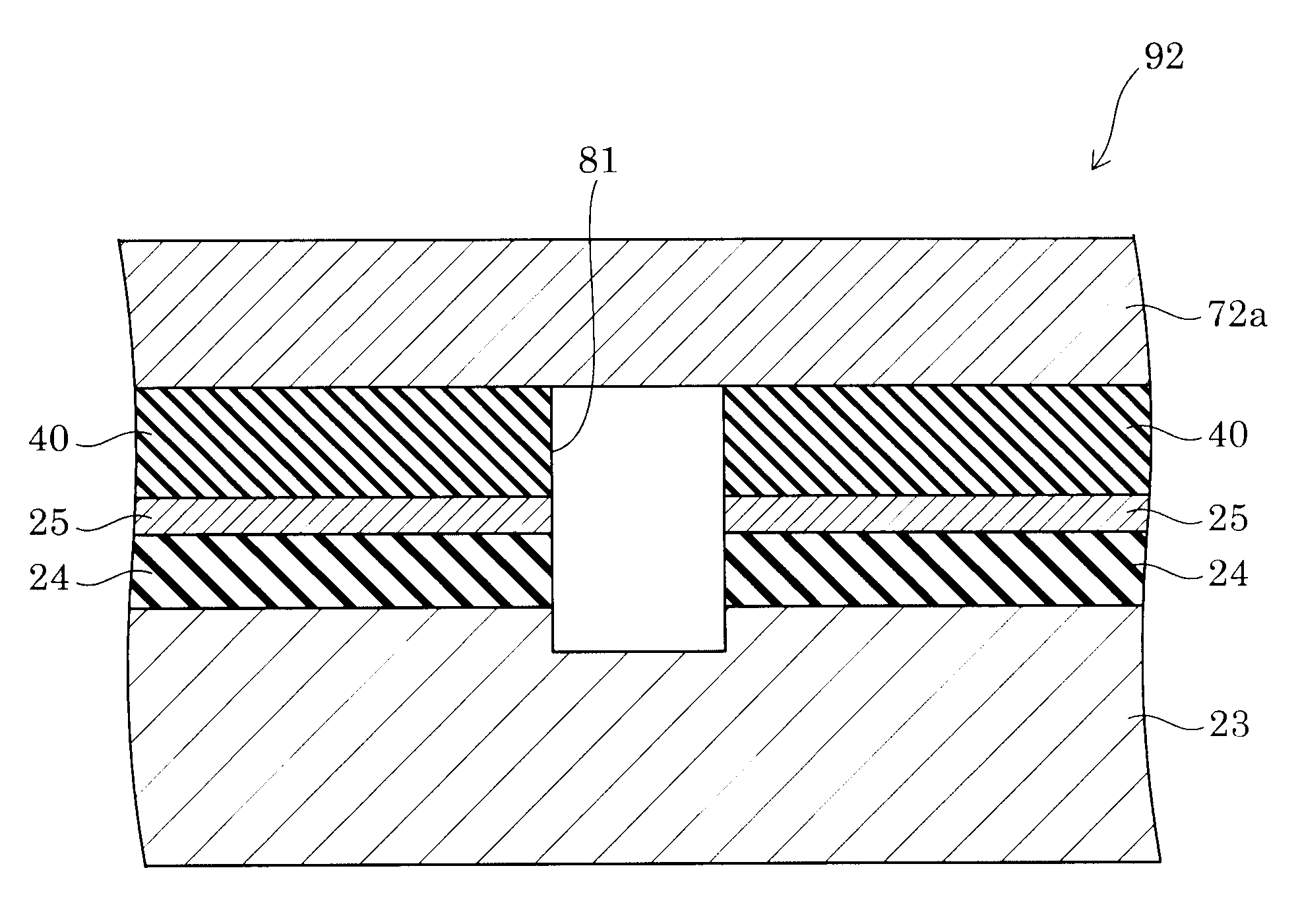
[0064]FIG. 7 is a cross-sectional view illustrating a semiconductor device according to this embodiment.
[0065]The cross-sectional view of FIG. 7 shows a MOSFET (metal oxide semiconductor field effect transistor), which is used in the radio frequency circuit 4 shown in FIG. 1 for conduction of a radio frequency signal (RF signal) having a frequency of 500 MHz or more and a power of 20 dBm or more. This MOSFET is formed on an SOI (silicon on insulator) substrate.
[0066]More specifically, the semiconductor device 21 includes an SOI (silicon on insulator) substrate 22. The SOI substrate 22 includes a P-type high-resistance silicon substrate 23 doped with boron (B) and having a specific resistance of 1 kΩ·cm or more. A BOX (buried oxide) layer 24 is provided as a silicon oxide film on the high-resistance silicon substrate 23, and a silicon layer 25 is provided on the BOX layer 24. The thickness of the BOX layer 24 is illustratively 2 μm, and the thic...
third embodiment
[0079]Next, the invention is described.
[0080]FIG. 10 is a plan view illustrating a semiconductor device according to this embodiment.
[0081]FIG. 11 is a circuit diagram illustrating the semiconductor device according to this embodiment.
[0082]The semiconductor device according to this embodiment is an example where the MOSFET shown in the above second embodiment is applied to a radio frequency switch circuit, and particularly to a shunt SPDT (single-pole double-throw) switch circuit.
[0083]As shown in FIG. 10, the semiconductor device 41 according to this embodiment includes an interlayer insulating film 40 formed on an SOI substrate. On the interlayer insulating film 40 are provided an antenna pad 42 to be connected to an antenna terminal; a transmit pad 43 to be connected to a first RF terminal, e.g., an RF terminal of an external transmitting circuit (not shown); a receive pad 44 to be connected to a second RF terminal, e.g., an RF terminal of an external receiving circuit (not show...
PUM
 Abstract
Description
Claims
Application Information