Quantum dot vertical cavity surface emitting laser and fabrication method of the same

a vertical cavity surface and laser technology, applied in the direction of lasers, semiconductor lasers, lasers, etc., can solve the problems of increasing the size of the vcsel device, difficult to control the wavelength compared to the quantum well structure, and limited dbr and other substrate materials, etc., to achieve excellent light emission efficiency and easy manufacturing

Inactive Publication Date: 2008-09-18
SAMSUNG ELECTRONICS CO LTD
View PDF16 Cites 12 Cited by
  • Summary
  • Abstract
  • Description
  • Claims
  • Application Information

AI Technical Summary

Benefits of technology

[0010]The present invention may provide a quantum dot vertical capacity surface emitting laser (QD-VCSEL) having excellent light emitting efficiency and the wavelength characteristic which is easily manufactured and a fabrication method of the same.

Problems solved by technology

However, when a quantum dot device is used, it is difficult to control the wavelength compared to the quantum well structure.
However, since the quantum layer is formed by a crystal method, in other words an epitaxal growth method, the possible material of DBR and the other substrate would be limited.
More specifically, since the refractive indexes of the material layers, which form the DBR, are small, the number of the material layers is increased, resulting in an increase in the size of the VCSEL device.
In addition, the manufacturing method and the manufacturing cost for the VCSEL device are increased.

Method used


Image

  • Quantum dot vertical cavity surface emitting laser and fabrication method of the same
  • Quantum dot vertical cavity surface emitting laser and fabrication method of the same
  • Quantum dot vertical cavity surface emitting laser and fabrication method of the same

Examples


Embodiment Construction

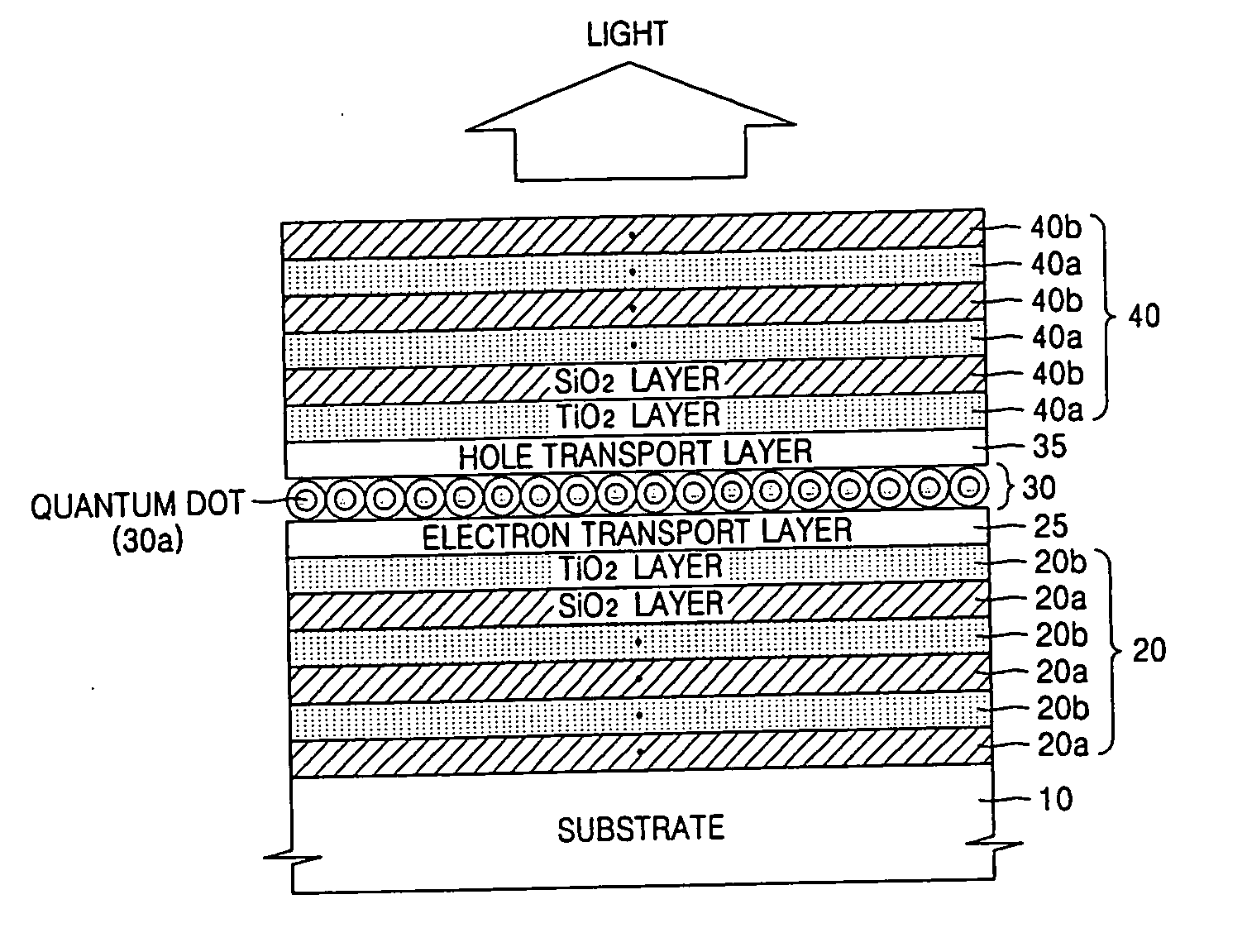
[0019]FIG. 1 is a sectional view of a quantum dot vertical capacity surface emitting laser (QD-VCSEL) according to an embodiment of the present invention.

[0020]Referring to FIG. 1, the QD-VCSEL device according to the embodiment includes a lower distributed brag reflector (DBR) mirror 20, an electron transport layer (ETL) 25, an emitting layer (EML) 30, a hole transport layer (HTL) 35, and an upper DBR mirror 40.

[0021]The substrate 10 can be formed of glass and sapphire, instead of semiconductor, and the material of the substrate 10 can vary as will be apparent to those of ordinary skill in the art.

[0022]The ETL 25 transports the electrons supplied from the cathode to the EML 30, and the ETL 25 is mainly formed by an Alq3 or TAZ material.

[0023]The HTL 35 transports the holes injected from an anode to the EML 30, and the HTL 35 is mainly formed by α-NPD or TPD material.

[0024]The electrons and the holes supplied from the cathode and the anode are recombined in the EML 30 to emit light...


PUM


Abstract

A quantum dot vertical capacity surface emitting laser (QD-VCSEL) and a method of manufacturing the same are provided. The QD-VCSEL includes a substrate, a lower distributed brag reflector (DBR) mirror formed on the substrate, an electron transport layer (ETL) formed on the lower DBR mirror, an emitting layer (EML) formed of nano-particle type group II-VI compound semiconductor quantum dots on the ETL, a hole transport layer (HTL) formed on the EML, and an upper DBR mirror formed on the HTL.

Description

CROSS-REFERENCE TO RELATED PATENT APPLICATION[0001]This application claims the benefit of Korean Patent Application No. 10-2005-0012419, filed on Feb. 15, 2005, in the Korean Intellectual Property Office, the disclosure of which is incorporated herein in its entirety by reference.BACKGROUND OF THE DISCLOSURE[0002]1. Field of the Disclosure[0003]The present disclosure relates to a quantum dot vertical cavity surface emitting laser and a fabrication method of the same, and more particularly, to a quantum dot vertical cavity surface emitting laser having an excellent light emitting efficiency and wavelength characteristic and ease of manufacture, and to a fabrication method of the same.[0004]2. Description of the Related Art[0005]Quantum dots may have well separated energy gaps and trap carriers in a three-dimensional arrangement, thus the quantum dot structure has excellent thermal stability when utilized as an optical device when compared to a quantum well structure. A self-assembled...

Claims


Application Information

Patent Timeline
Patent Type & Authority Applications(United States)
IPC IPC(8): H01L33/00B82Y20/00
CPCB82Y20/00H01S5/026H01S5/34H01S5/18H01S5/041E02D5/765E02D5/80E02D2600/30
Inventor LEE, EUN-KYUNGCHOI, BYOUNG-LYONG
Owner SAMSUNG ELECTRONICS CO LTD
Why Eureka
Try Eureka