Powdered quantum dots

a quantum dots and quantum technology, applied in the field of quantum dots, can solve the problems of quantum dots no longer showing the optical or electronic properties of their bulk parent semiconductor, quantum yields are greatly reduced, and quantum yields of quantum dots are greatly and irreversibly diminished

Inactive Publication Date: 2008-09-25
SAMSUNG ELECTRONICS CO LTD
View PDF5 Cites 93 Cited by
  • Summary
  • Abstract
  • Description
  • Claims
  • Application Information

AI Technical Summary

Benefits of technology

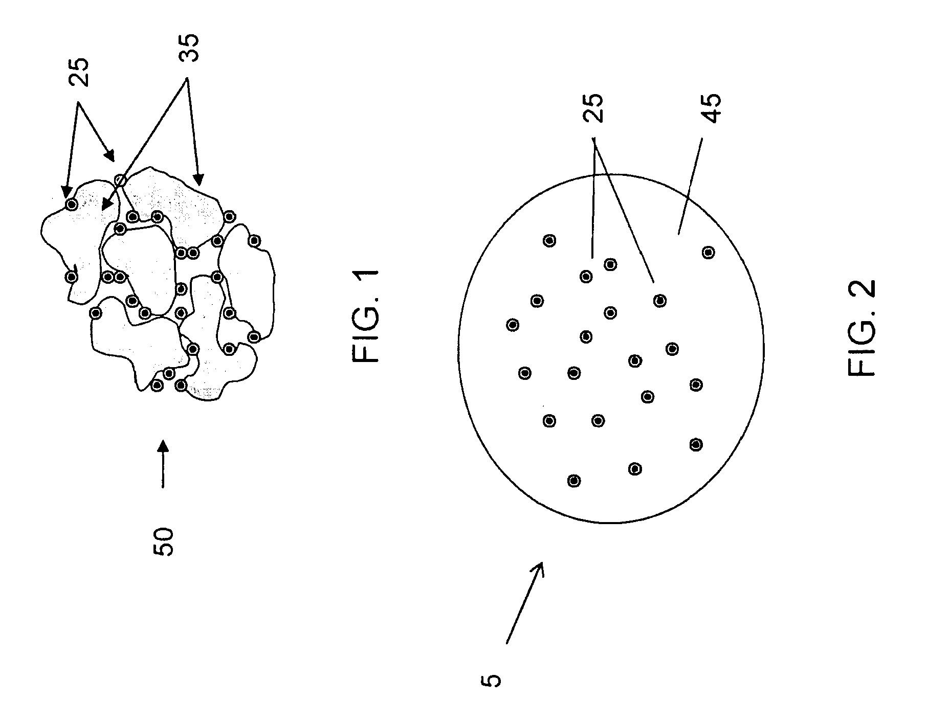
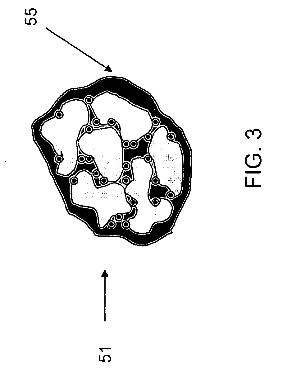
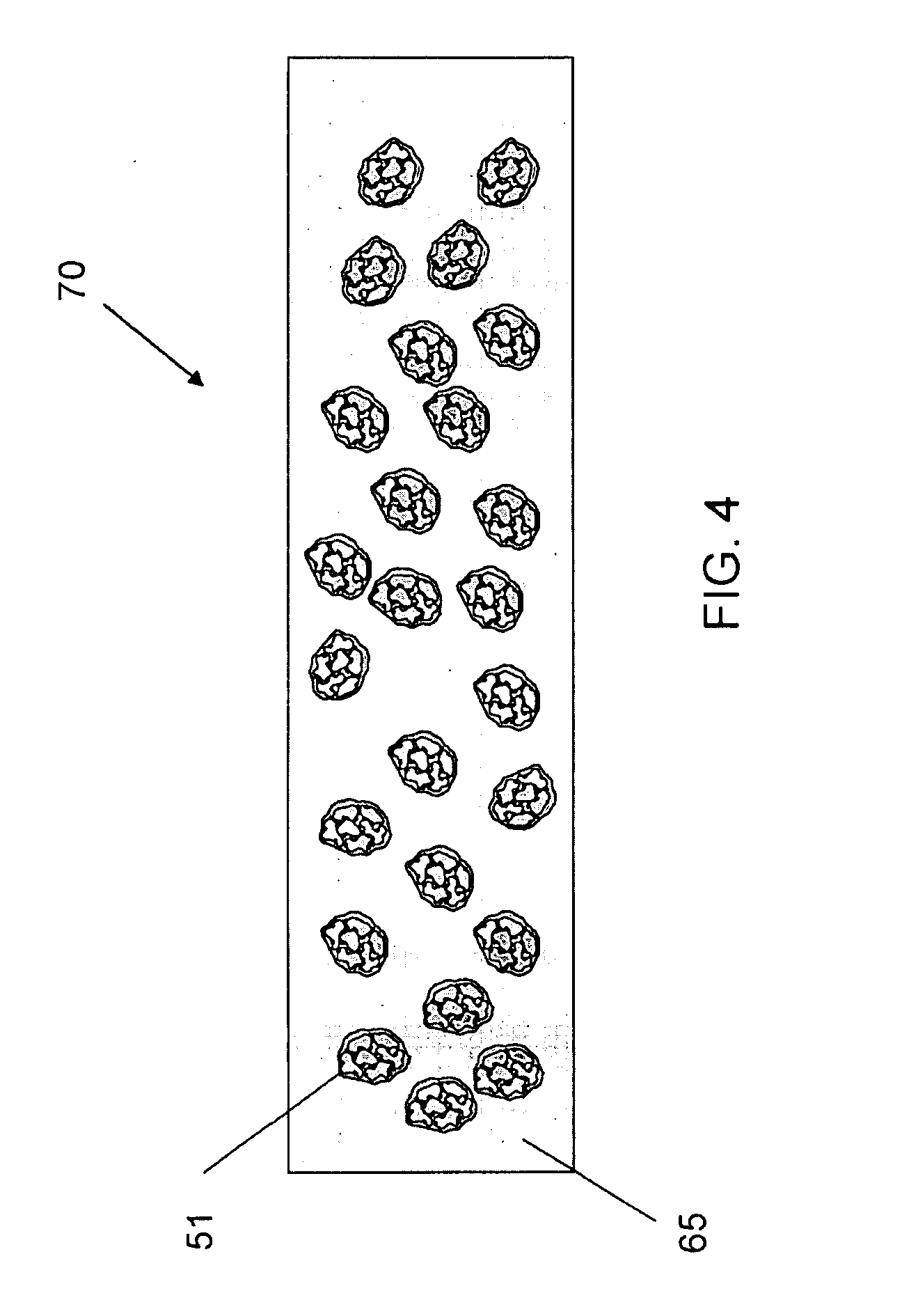
[0018]In certain embodiments, the quantum dot particle is coated with a dielectric layer to protect the quantum dots from photooxidation as well as to allow the quantum dots to be compatible with agents that are used to form silicone materials for example.

Problems solved by technology

As a consequence, quantum dots no longer exhibit the optical or electronic properties of their bulk parent semiconductor.
Any macroscopic collection of nanocrystals, however, emits a line that is inhomogeneously broadened due to the fact that every collection of nanocrystals is unavoidably characterized by a distribution of sizes.
Non-radiative exciton recombination reduces quantum yield due to the presence of interband states resulting from dangling bonds at the quantum dot surface and intrinsic defects.
The overall result is that in certain chemically reactive and photoxidative environments the quantum yields of the quantum dots are greatly and irreversibly diminished.
Furthermore, sulfur atoms, which are one component of zinc sulfide shells that are frequently used to passivate nanocrystal cores, as well as amine moieties, which is often a component of the surfactant layer that envelopes the nanocrystal cores, may adversely affect the matrix material in which the quantum dots are dispersed.
However, these particles suffer drawbacks.
Further, many organic materials have relatively low melting points or may degrade at elevated temperatures.

Method used


Image

  • Powdered quantum dots
  • Powdered quantum dots
  • Powdered quantum dots

Examples


example 1

Using Fumed Silica as the Dielectric Material

[0044]The quantum dots (100 mg in 5 mL toluene) were washed once with methanol and resuspended in 20 mL anhydrous toluene. To the suspension was added to 1 gram of fumed silica and the mixture was sonicated for 4 hours. The solvent was removed by evaporation. The resulting powder was optionally washed with methanol and optionally milled to size under 5 microns. The size was approximated using a microscope.

example 2

Using Alumina as the Dielectric Material

[0045]The same procedure as in Example 1 was followed, except that alumina was used instead of fumed silica. It has been observed that less quantum dots were absorbed to alumina particles than to fumed silica particles by visual observation of the luminescence.

example 3

Using Colloidal Silica as the Dielectric Material

[0046]150 mL of water was added to 1.7 g of colloidal silica (LUDOX LS, 30% silica in water by mass, from Grace Davison) while stirring rapidly. 50 mg of quantum dots were suspended in 10 mL of anhydrous toluene. The suspension was added to the colloidal silica solution. Colloidal silica (in solution). The mixture was left in a fume hood under stirring for 4 hours while allowing solvent to evaporate to a final volume of 45 ml. Precipitates formed from the mixture were separated out by centrifugation. 1.09 g of product was obtained and dried in air. The resultant product was a brittle fluorescent material which was ground into a fine powder using a mortar and pestle.

Quantum Dot Particles Comprising Quantum Dot-Crosslinked Silane Complex:


PUM

PropertyMeasurementUnit
diameteraaaaaaaaaa
diameteraaaaaaaaaa
physical sizeaaaaaaaaaa

Abstract

Powdered quantum dots that can be dispersed into a silicone layer are provided. The powdered quantum dots are a plurality of quantum dot particles, preferably on the micron or nanometer scale. The powdered quantum dots can include quantum dot-dielectric particle complexes or quantum dot-crosslinked silane complexes. The powdered quantum dots can included quantum dot particles coated with a dielectric layer.

Description

CROSS-REFERENCE TO RELATED APPLICATION[0001]The present application claims priority to U.S. Provisional Application No. 60 / 918,927, filed on Mar. 20, 2007, which is incorporated by reference herein.TECHNICAL FIELD[0002]The present invention relates to powdered quantum dots and methods of making and using the same.BACKGROUND[0003]Quantum dots (QDs) comprise colloidal semiconductor cores that are small, often spherical, crystalline particles composed of group II-VI, III-V, IV-VI, or I-III-VI semiconductor materials. Each semiconductor core is a nanocrystal consisting of hundreds to thousands of atoms. Quantum dots are neither atomic nor bulk semiconductors, but may best be described as artificial atoms. Their properties originate from their physical size, which ranges from about 1 to about 10 nanometers (nm) in radius, and are often comparable to or smaller than the bulk Bohr exciton radius. As a consequence, quantum dots no longer exhibit the optical or electronic properties of their...

Claims


Application Information

Patent Timeline
Patent Type & Authority Applications(United States)
IPC IPC(8): H01B1/00
CPCB82Y30/00C09K11/02H01L21/02601C09K11/641H01L21/02521C09K11/592
Inventor GILLIES, JENNIFERSOCHA, DAVIDLOCASCIO, MICHAEL
Owner SAMSUNG ELECTRONICS CO LTD
Why Eureka
Try Eureka