Method of fabricating two-step self-aligned contact
- Summary
- Abstract
- Description
- Claims
- Application Information
AI Technical Summary
Benefits of technology
Problems solved by technology
Method used
Image

Examples
first embodiment
The First Embodiment
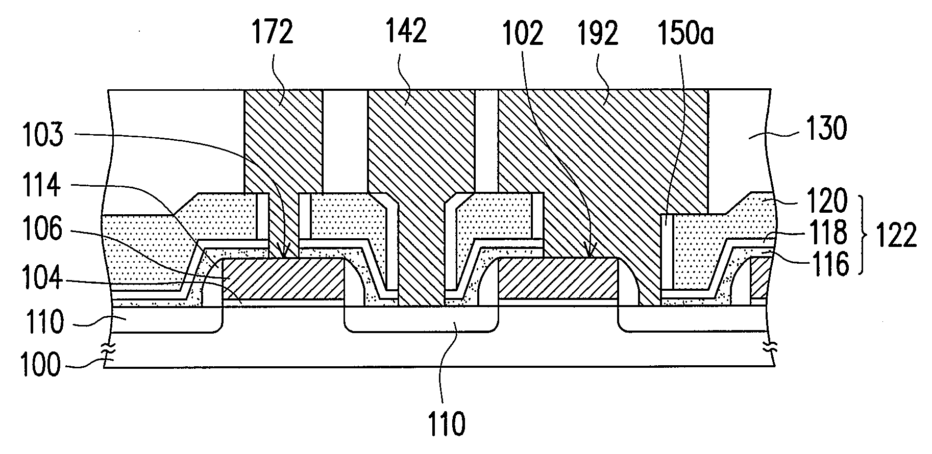
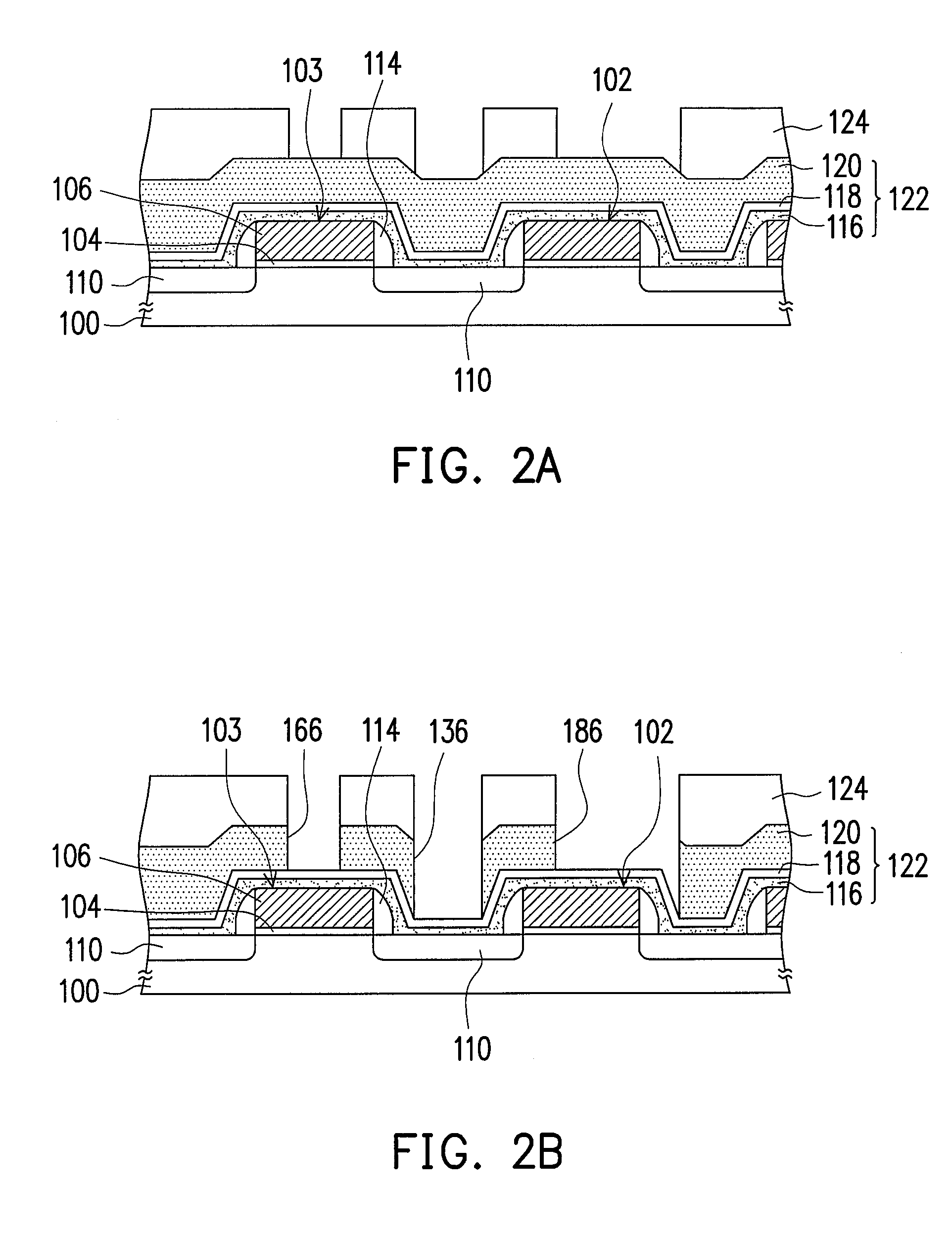
[0044]FIGS. 2A-2F are sectional views of the processes of a method of fabricating a semiconductor device according to an embodiment of the present invention.
[0045]Referring to FIG. 2A, a substrate 100 is provided first. The substrate 100 is, for example, a silicon substrate, such as an n-type silicon substrate or a p-type silicon substrate. Definitely, the substrate 100 can also be a silicon-on-insulator (SOI) substrate. Transistors 102 and 103 are already formed on the substrate 100, which are for example, n-channel metal-oxide-semiconductors (NMOS) or p-channel metal-oxide-semiconductors (PMOS).
[0046]The transistors 102 and 103 respectively include a gate dielectric layer 104, a gate 106, a spacer 114, and a source / drain 110. The gate dielectric layer 104 is disposed between the gate 106 and the substrate 100. The material of the gate dielectric layer 104 is constituted of silicon oxide layer. The material of the gate 106 includes a silicon-based material, for ...
second embodiment
The Second Embodiment
[0063]FIGS. 3A-3H are sectional views of the processes of a method of fabricating another semiconductor device according to an embodiment of the present invention.
[0064]Referring to FIGS. 3A and 3B, a first stage of patterning process is performed on the dielectric layer 122 on the substrate 100 according to the method of the first embodiment, so as to form a lower hole 136 corresponding to the source / drain region 110, a lower hole 166 corresponding to the gate 106 of the transistor 103, and a lower hole 186 corresponding to the gate 106 of the transistor 102 and the source / drain region 110 of the transistor 103 in the dielectric layer 122.
[0065]Referring to FIG. 3C, after removing the photoresist layer 124, a conformal liner layer material layer 150 is formed on the substrate 100 for covering the dielectric layer 122 and the sidewalls and bottoms of the lower holes 136, 166, and 186. The material of the liner layer material layer 150 includes silicon oxide or s...
PUM
 Abstract
Description
Claims
Application Information