Electrode structure for fringe field charge injection

a charge injection and electrode technology, applied in the field of electrode electrode structures, can solve the problems of low work function metals, such as calcium, which are very susceptible to oxidation and may be easily damaged, and achieve the effect of improving charge injection into semiconductor materials

Inactive Publication Date: 2008-10-02
PANASONIC CORP +1
View PDF8 Cites 5 Cited by
  • Summary
  • Abstract
  • Description
  • Claims
  • Application Information

AI Technical Summary

Benefits of technology

[0005]The present invention provides an alternative electrode structure that may provide improved charge injection into semiconductor materials of electronic devices.

Problems solved by technology

In particular, the performance of organic semiconductor devices, such as organic light emitting diodes (OLED's) and polymer light emitting diodes (PLED's), has been limited by the relatively high charge injection resistance of organic semiconductor materials.
Low work function metals, such as, for example, calcium, are very susceptible to oxidation and may be easily damaged by air or humidity.
Thus, the use of electrodes formed of such materials may necessitate incorporating, potentially complex, encapsulation structures in the design and manufacture of these devices.
However, in some devices the level of doping used to form an ohmic contact may be undesirable, particularly if the dopants may be capable of significant diffusion during operation.

Method used


Image

  • Electrode structure for fringe field charge injection
  • Electrode structure for fringe field charge injection
  • Electrode structure for fringe field charge injection

Examples


Embodiment Construction

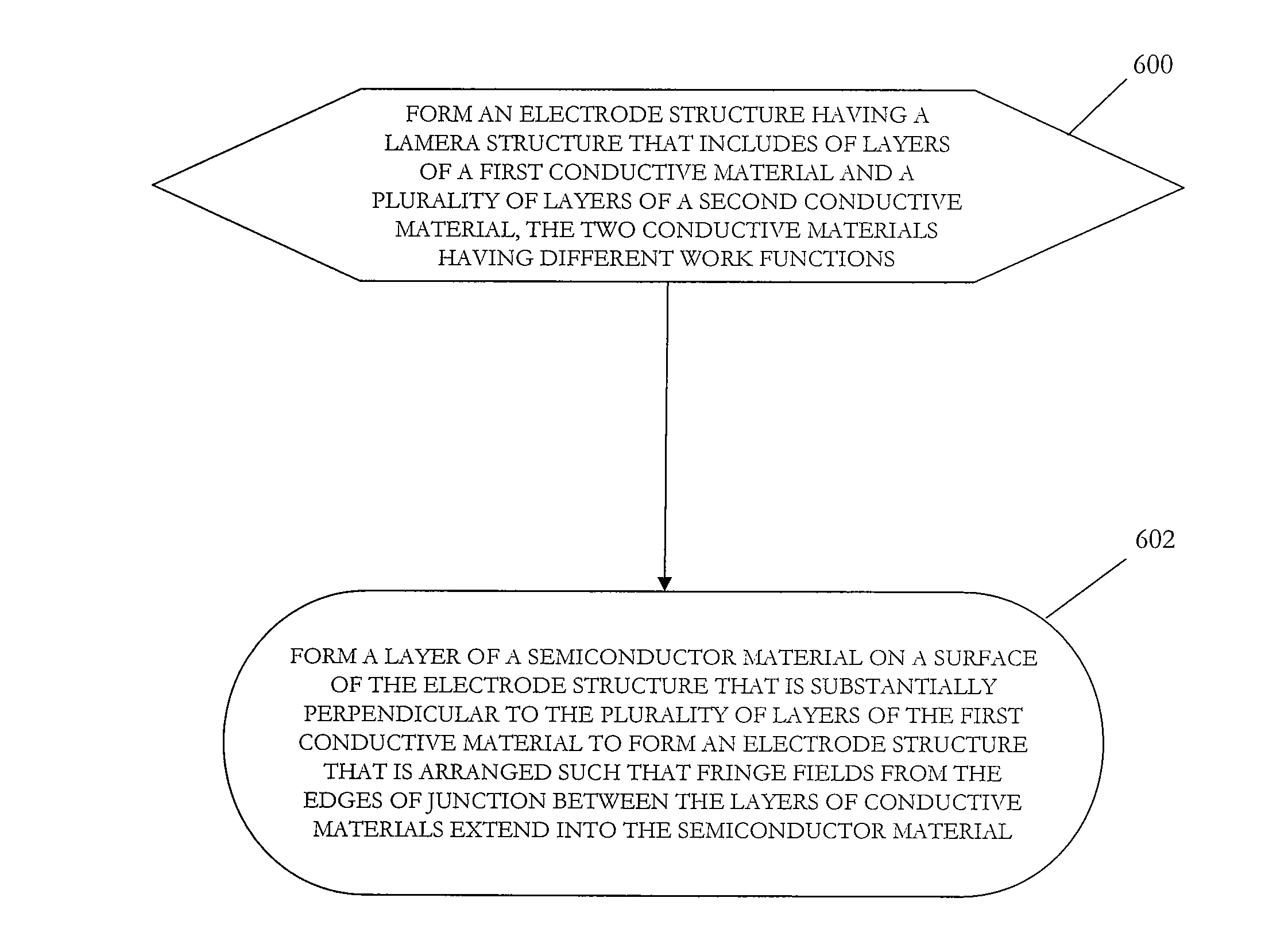
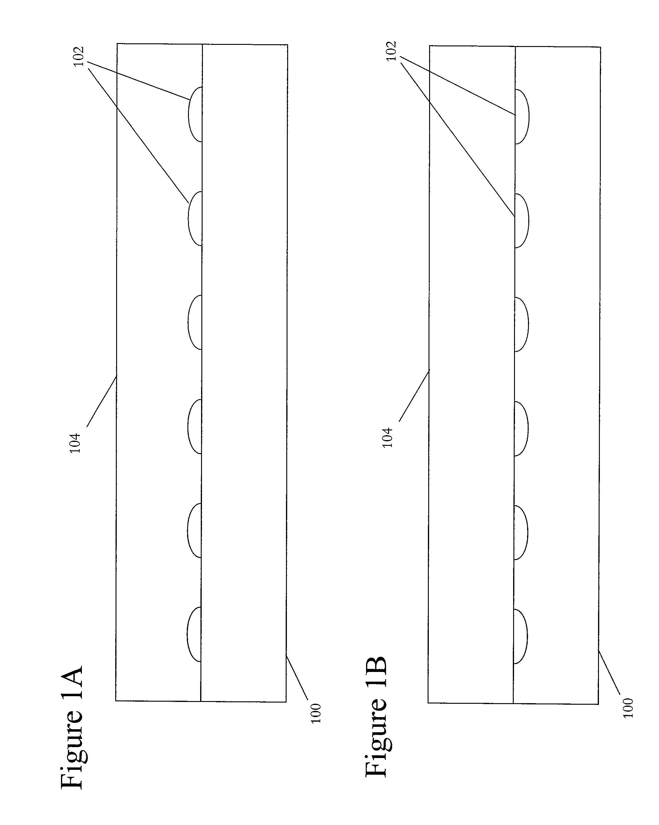
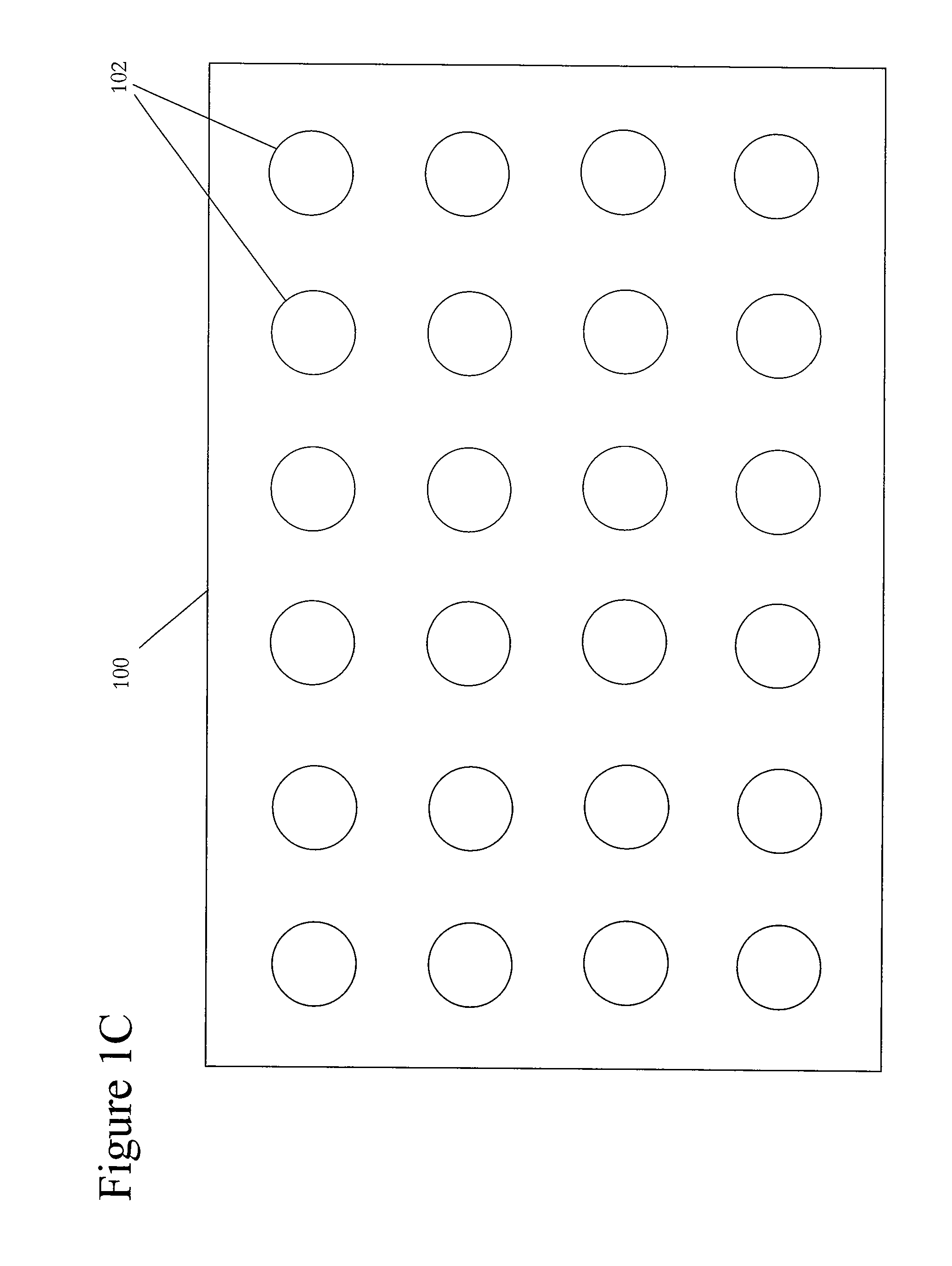
[0019]Exemplary embodiments of the present invention use two different conductors that have different work functions (WF's) to enhance charge injection into semiconductor devices, such as electroluminescent (EL) or thin film transistor (TFT) devices. These exemplary embodiments may also be used to enhance charge extraction from semiconductor devices, such as photovoltaic detectors and solar cells. The exemplary electrode structure formed by these two conductive materials creates a fringe field at the edge of the interface, or junction, between the two conductors. The resulting fringe field may improve charge injection into adjacent regions of semiconductor material. If the ratio of the length of such junction edges to the surface area of the electrode to semiconductor contact is sufficiently high, the resulting charge injection enhancement may be significant. This ratio may be increased by creating small islands of one of the conductors on the electrode contact surface, possibly eve...


PUM


Abstract

A semiconductor device, including: a semiconductor material and an electrode structure electrically coupled to the semiconductor material. The electrode structure includes: a first portion formed of a first conductive material and a second portion formed of a second conductive material. Both the first portion and the second portion of the electrode structure are in direct contact with the semiconductor material. The first conductive material has a first work function and the second conductive material has a second work function that is different from the first work function, so that the second portion of the electrode structure forms a junction with the first portion. The first portion and the second portion of the electrode structure are arranged such that the fringe field from the edge of this junction between the first portion and the second portion extends into the semiconductor material.

Description

FIELD OF THE INVENTION[0001]The present invention concerns electrode structures designed to provide fringe field charge injection. These electrode structures may allow for the manufacture of improved and / or simplified electronic devices.BACKGROUND OF THE INVENTION[0002]Charge injection into the semiconductor materials of electronic devices plays a significant role in device efficiency, as well as device quality.[0003]In particular, the performance of organic semiconductor devices, such as organic light emitting diodes (OLED's) and polymer light emitting diodes (PLED's), has been limited by the relatively high charge injection resistance of organic semiconductor materials. To overcome the charge injection resistance, low work function metals are typically used in organic semiconductor devices. These metals improve charge injection. Low work function metals, such as, for example, calcium, are very susceptible to oxidation and may be easily damaged by air or humidity. Thus, the use of ...

Claims


Application Information

Patent Timeline
Patent Type & Authority Applications(United States)
IPC IPC(8): H01L29/76H01L21/339
CPCB82Y20/00B82Y30/00H01L31/0224H01L51/5203H01L51/5221H01L2251/5369H01L51/5225
Inventor MALLIARAS, GEORGE G.MORI, KIYOTAKAFONG, HON HANG
Owner PANASONIC CORP
Why Eureka
Try Eureka