Semiconductor device and electronic device

Active Publication Date: 2008-10-02
SEMICON ENERGY LAB CO LTD
View PDF33 Cites 32 Cited by
  • Summary
  • Abstract
  • Description
  • Claims
  • Application Information

AI Technical Summary

Benefits of technology

[0016]When the present invention is used, electrostatic discharge can be suppressed without changing the size of an optical

Problems solved by technology

A current mirror circuit is formed using a transistor; however, there is a case where an electrode or a transistor is damag

Method used


Image

  • Semiconductor device and electronic device
  • Semiconductor device and electronic device
  • Semiconductor device and electronic device

Examples


embodiment mode 1

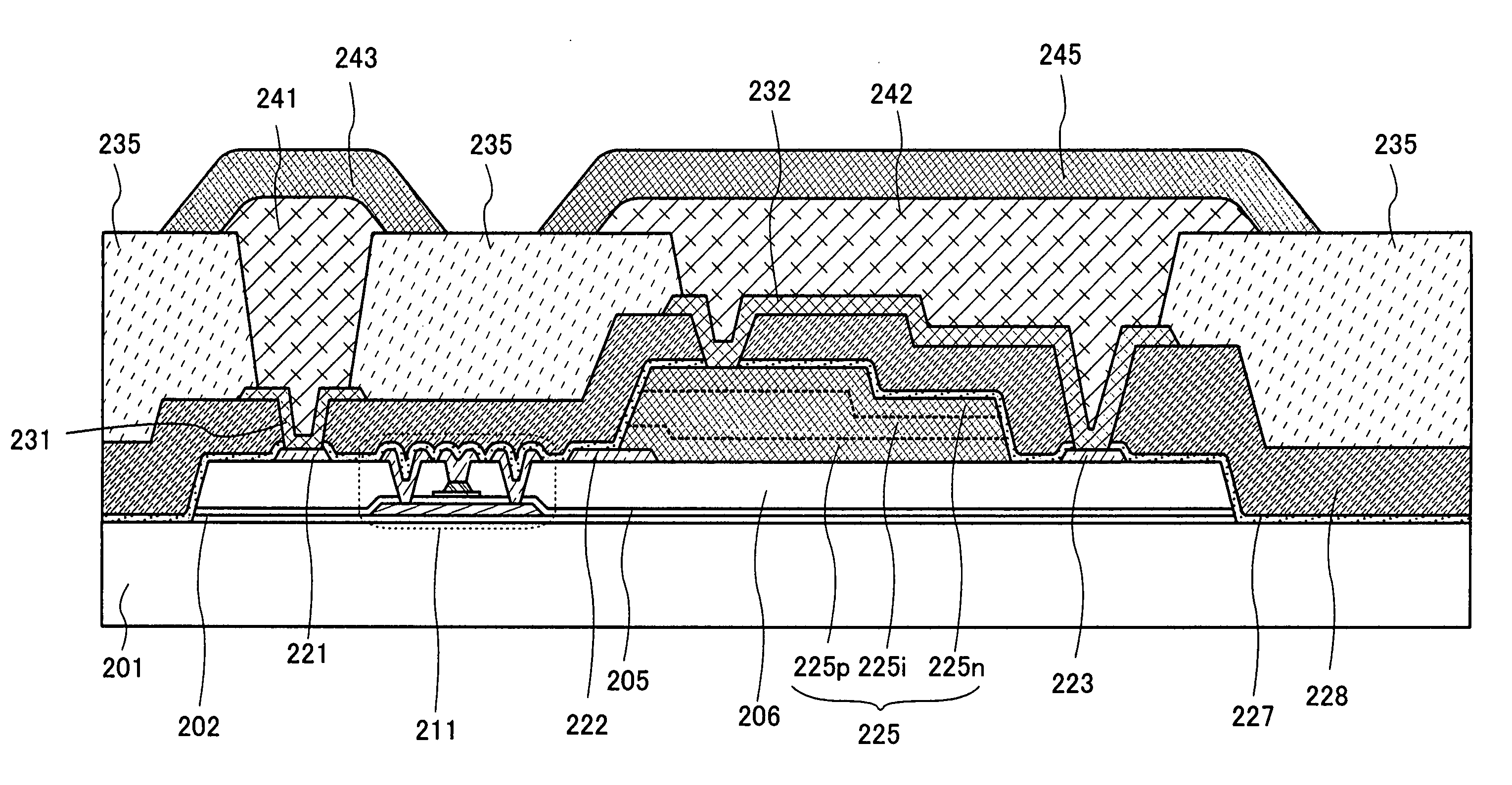
[0039]A photoelectric conversion device of this embodiment mode is described below with reference to FIG. 1, FIG. 2, FIG. 3, FIG. 4, FIGS. 5A to 5C, FIGS. 6A to 6C, FIGS. 7A and 7B, FIG. 8, FIG. 9, and FIG. 10.

[0040]First, as shown in FIG. 3, a photoelectric conversion device 100 of this embodiment mode includes a photodiode 103 and a current mirror circuit 101 which is an amplifier circuit amplifying output current of the photodiode 103. The current mirror circuit 101 includes thin film transistors (TFTs) 104 and 105.

[0041]In this embodiment mode, n-channel TFTs are used as the TFTs 104 and 105. In the current mirror circuit 101, the same voltage is applied to gate portions of the reference-side TFT 104 and the output-side TFT 105 to control current flowing through the output-side TFT 105 based on current flowing through the reference-side TFT 104.

[0042]In FIG. 3, a gate electrode of the TFT 104 included in the current mirror circuit 101 is electrically connected to a gate electrod...

embodiment mode 2

[0108]In this embodiment mode, a photoelectric conversion device having a structure which is different from that of Embodiment Mode 1 is described with reference to FIG. 11, FIGS. 12A and 12B, and FIG. 19.

[0109]Note that like portions in this embodiment mode and Embodiment Mode 1 are denoted by the same reference numerals based on the description of Embodiment Mode 1.

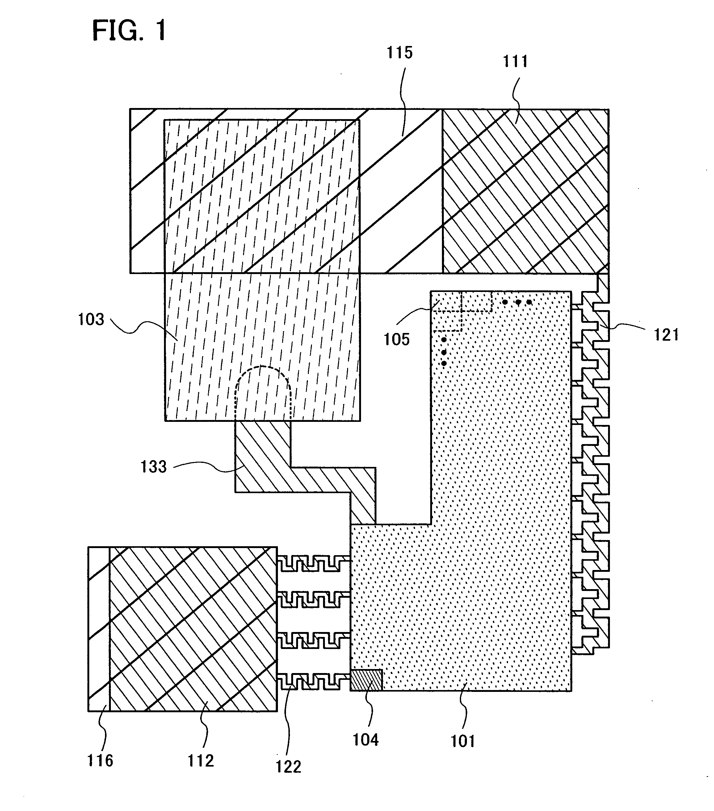
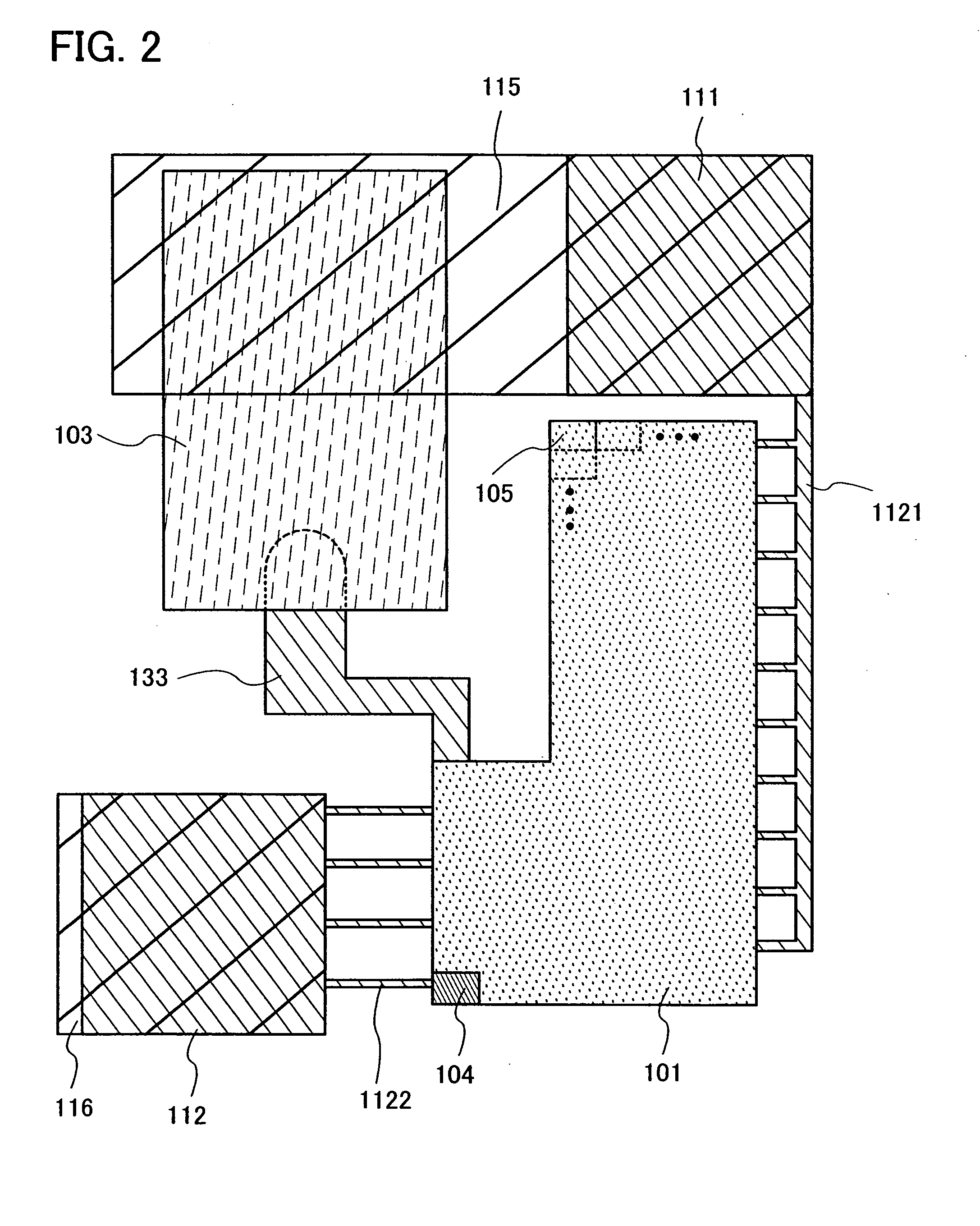
[0110]FIG. 11 shows a photoelectric conversion device of this embodiment mode. FIG. 11 of this embodiment mode is different from FIG. 1 of Embodiment Mode 1 in that an electrode 401 is formed over the wiring 121 and an electrode 402 is formed over the wiring 122.

[0111]When the electrode 401 and the electrode 402 are formed, resistance values of the resistor 113 and the resistor 114, which are wiring resistance, are increased. Thus, electrostatic discharge can be further suppressed.

[0112]FIG. 12A shows a cross section taken along line A-A′ in FIG. 11. The wiring 121 is formed over the insulating film 202 which is over th...

embodiment mode 3

[0116]In this embodiment, examples are described in which photoelectric conversion devices obtained in Embodiment Modes 1 and 2 are incorporated in various electronic devices. As examples of electronic devices shown in this embodiment mode, a computer, a display, a mobile phone, a television receiver, and the like can be given. Specific examples of those electronic devices are shown in FIG. 13, FIGS. 14A and 14B, FIGS. 15A and 15B, FIG. 16, and FIGS. 17A and 17B.

[0117]FIG. 13 is a mobile phone, which includes a main body (A) 701, a main body (B) 702, a housing 703, operation keys 704, an audio input portion 705, an audio output portion 706, a circuit substrate 707, a display panel (A) 708, a display panel (B) 709, a hinge 710, a light-transmitting material portion 711, and an photoelectric conversion device 712 which is obtained in Embodiment Modes 1 and 2.

[0118]The photoelectric conversion device 712 detects light which is transmitted through the light-transmitting material portion...


PUM


Abstract

The present invention relates to a semiconductor device which includes a photoelectric conversion layer; an amplifier circuit amplifying an output current of the photoelectric conversion layer and including two thin film transistors; a first terminal supplying a high-potential power supply voltage; a second terminal supplying a low-potential power supply voltage; an electrode electrically connecting the two thin film transistors and the photoelectric conversion layer; a first wiring electrically connecting the first terminal and a first thin film transistor which is one of the two thin film transistors; and a second wiring electrically connecting the second terminal and a second thin film transistor which is the other of the two thin film transistors. In the semiconductor device, the value of voltage drop of the first wiring and the second wiring are increased by bending the first wiring and the second wiring.

Description

BACKGROUND OF THE INVENTION[0001]1. Field of the Invention[0002]The present invention relates to a semiconductor device having a photoelectric conversion element. In particular, the present invention relates to a semiconductor device having a photoelectric conversion element formed using a thin film semiconductor element and a manufacturing method thereof. Further, the present invention relates to an electronic device using the semiconductor device having the photoelectric conversion element.[0003]2. Description of the Related Art[0004]A large number of photoelectric conversion devices generally used for detecting electromagnetic waves are known, and for example, photoelectric conversion devices having sensitivity to ultraviolet rays to infrared rays are referred to as optical sensors (also referred to as photo sensors). Among optical sensors, an optical sensor having sensitivity to a visible light region with a wavelength of 400 to 700 nm is particularly referred to as a visible li...

Claims


Application Information

Patent Timeline
IPC IPC(8): H01L31/14G01J1/32
CPCH01L23/60H01L27/14H01L2924/09701H01L2924/0002H01L2924/00H01L31/10
Inventor SHISHIDO, HIDEAKI
Owner SEMICON ENERGY LAB CO LTD
Why Eureka
Try Eureka