

Semiconductor device package with die receiving through-hole and dual build-up layers over both side-surfaces for wlp and method of the same
a technology of semiconductor devices and build-up layers, which is applied in the direction of semiconductor devices, semiconductor/solid-state device details, electrical devices, etc., can solve the problems of time-consuming manufacturing process techniques, and inability to meet the demand of producing smaller chips with high-density elements on the chip. achieve good cte matching performance and improve board level reliability
- Summary
- Abstract
- Description
- Claims
- Application Information
AI Technical Summary
Benefits of technology
Problems solved by technology
Method used
Image

Examples
Embodiment Construction
[0023]The invention will now be described in greater detail with preferred embodiments of the invention and illustrations attached. Nevertheless, it should be recognized that the preferred embodiments of the invention is only for illustrating. Besides the preferred embodiment mentioned here, present invention can be practiced in a wide range of other embodiments besides those explicitly described, and the scope of the present invention is expressly not limited expect as specified in the accompanying Claims.
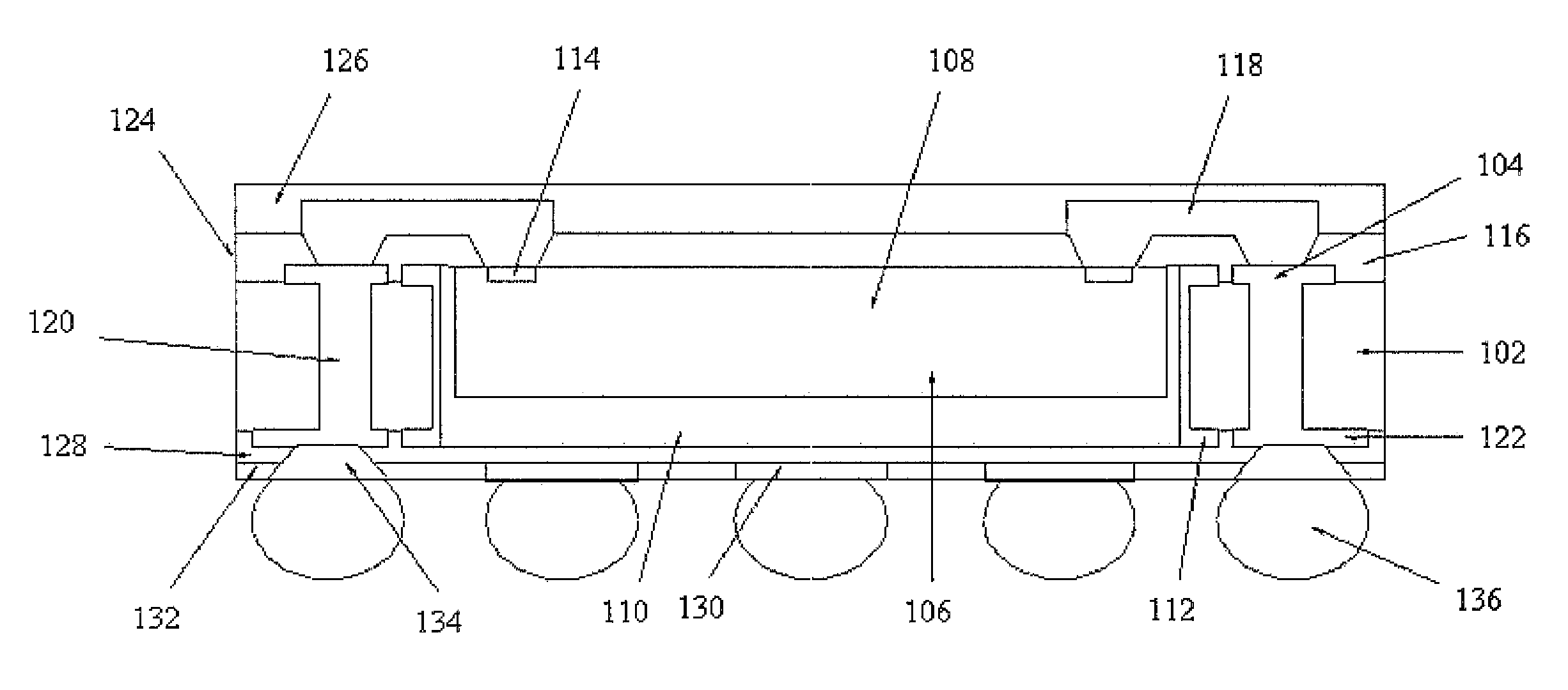
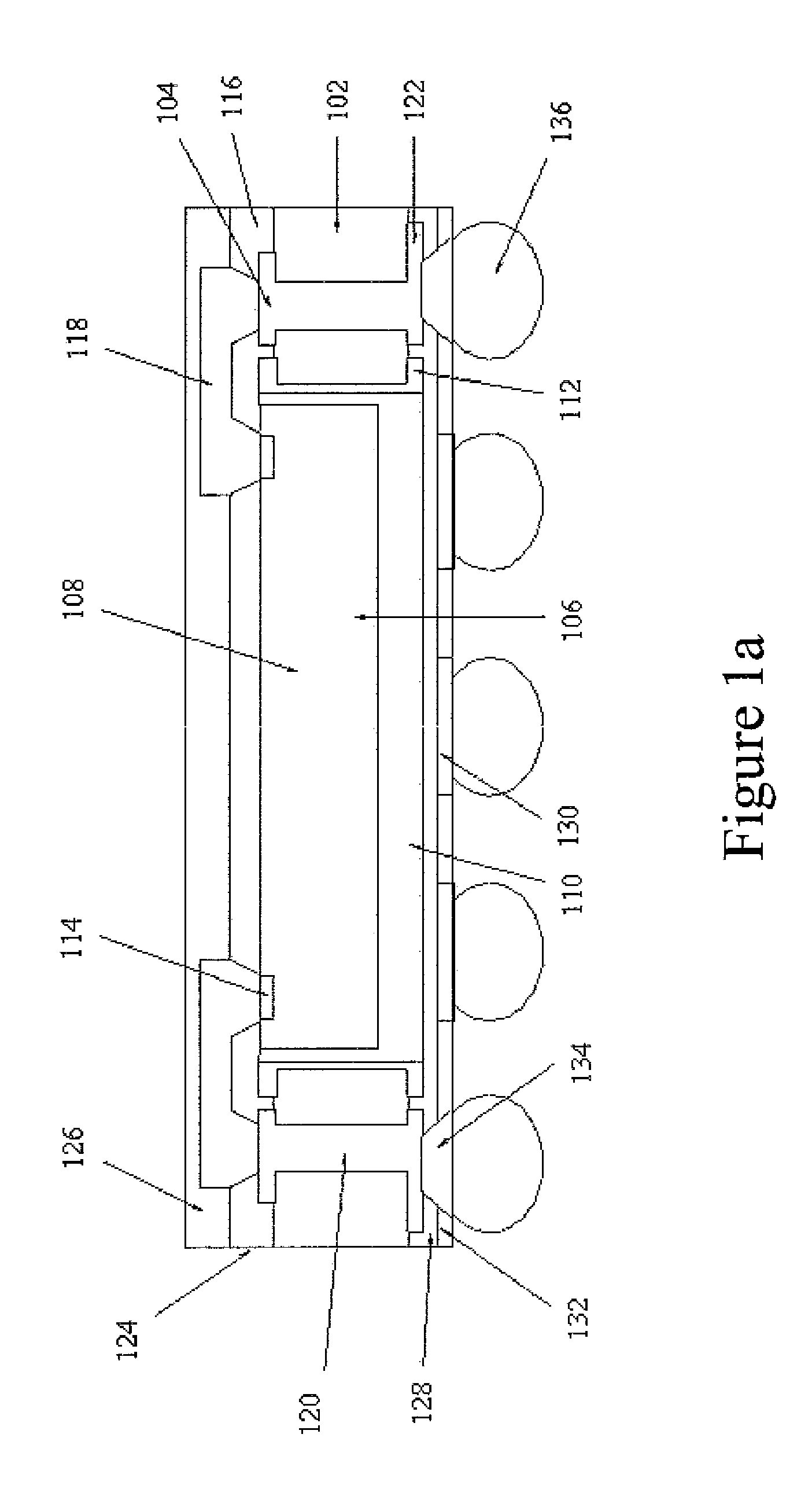
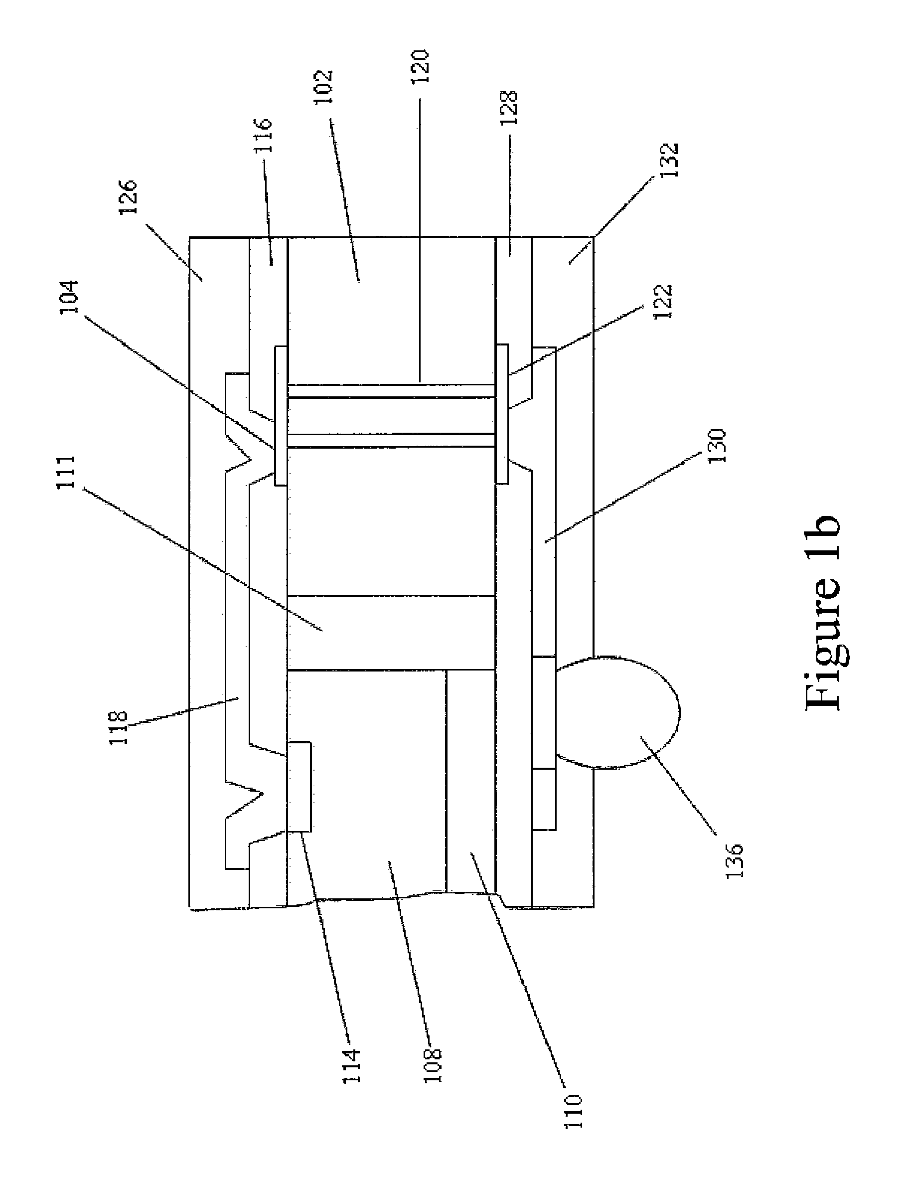
[0024]Referring to FIG. 1a, the present invention discloses a structure of fan-out WLP utilizing a substrate having predetermined contact metal pads 104 formed thereon and a pre-formed die receiving through holes 106 formed within the substrate 102. The substrate 102 is penetrated from upper surface to lower surface to form the die receiving through holes. At least a die with metal pads is disposed within the die receiving through hole of the substrate and attached by second (core...
PUM
 Abstract
Description
Claims
Application Information