Power semiconductor module, and power semiconductor device having the module mounted therein

a technology of power semiconductor and module, which is applied in the direction of semiconductor devices, semiconductor device details, semiconductor/solid-state devices, etc., can solve the problems of limited operating current range and efficient conductivity, and achieve the effect of inhibiting the generation of any voids

Inactive Publication Date: 2008-10-02
NICHICON CORP
View PDF4 Cites 71 Cited by
  • Summary
  • Abstract
  • Description
  • Claims
  • Application Information

AI Technical Summary

Benefits of technology

[0017]In the steps of soldering, first, the air in the vacuum reflow furnace is replaced by N2, and the temperature is raised to a point immediately below the melting point of solder. Then, by keeping that state for a predetermined period of time, internal temperatures of the finned base plate 3 and the insulated substrates 9 are equalized, and the soldering foils 12 are softened. Next, N2 in the vacuum reflow furnace is discharged to reduce the degree of vacuum to several kPa, and thereafter the vacuum reflow furnace is kept at a temperature higher than the melting point of solder for a predetermined period of time, thereby melting the solder. The pressure reduction at the time of melting the solder is intended to purge air bubbles ...

Problems solved by technology

However, the conventional power semiconductor device 1 shown in FIG. 2 has three problems specified below.
If any voids are generated, heat generated by the power semiconductor elements 8 cannot be ef...

Method used


Image

  • Power semiconductor module, and power semiconductor device having the module mounted therein
  • Power semiconductor module, and power semiconductor device having the module mounted therein
  • Power semiconductor module, and power semiconductor device having the module mounted therein

Examples


first embodiment

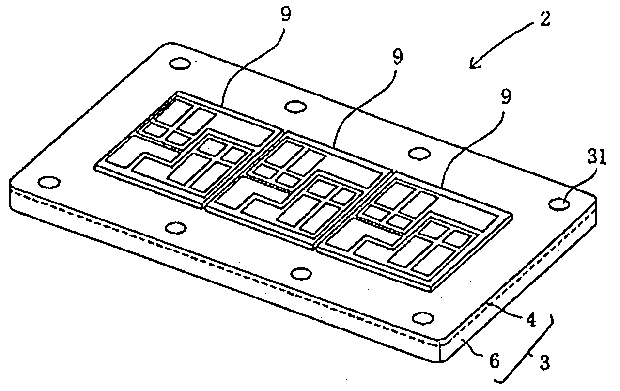
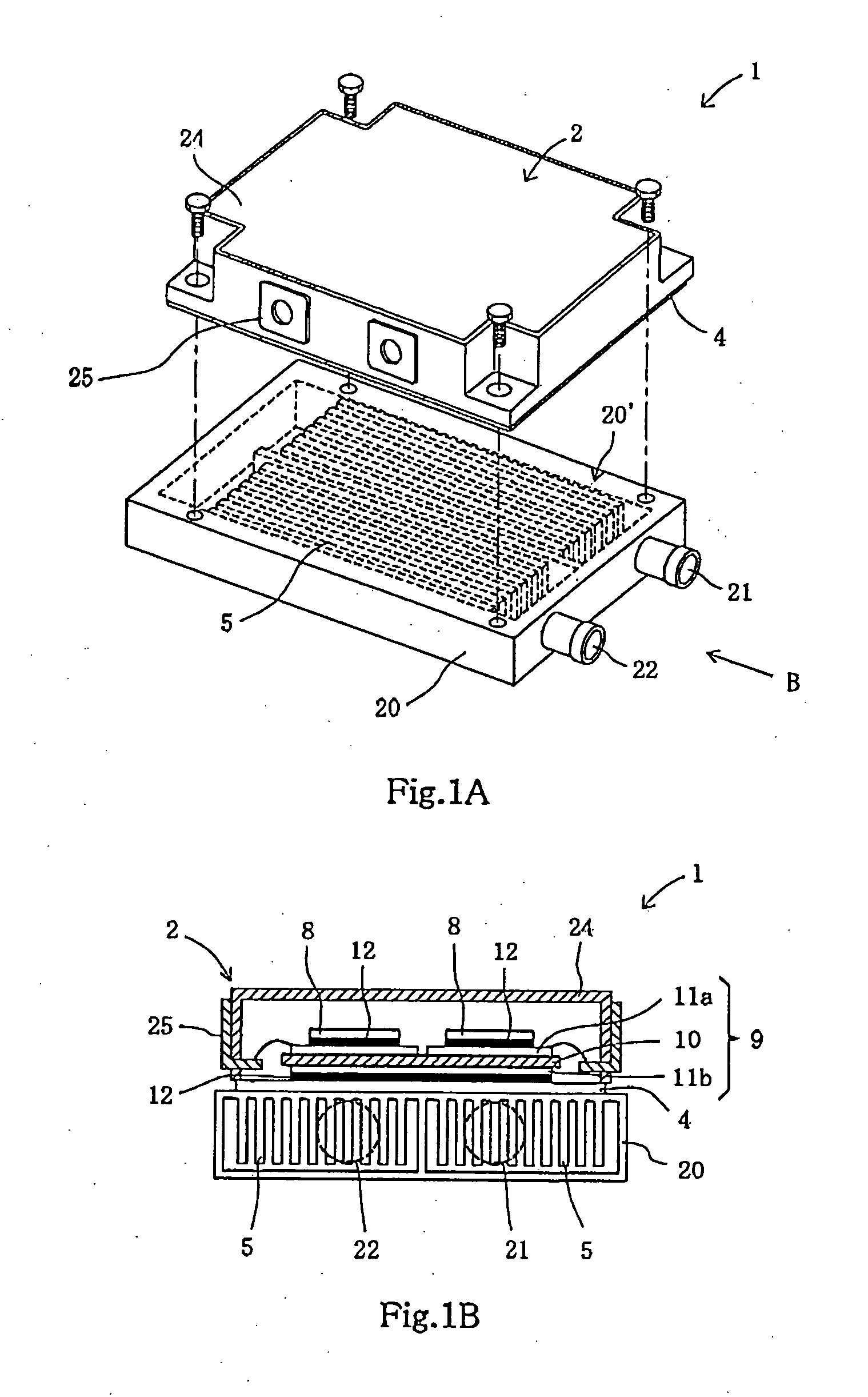
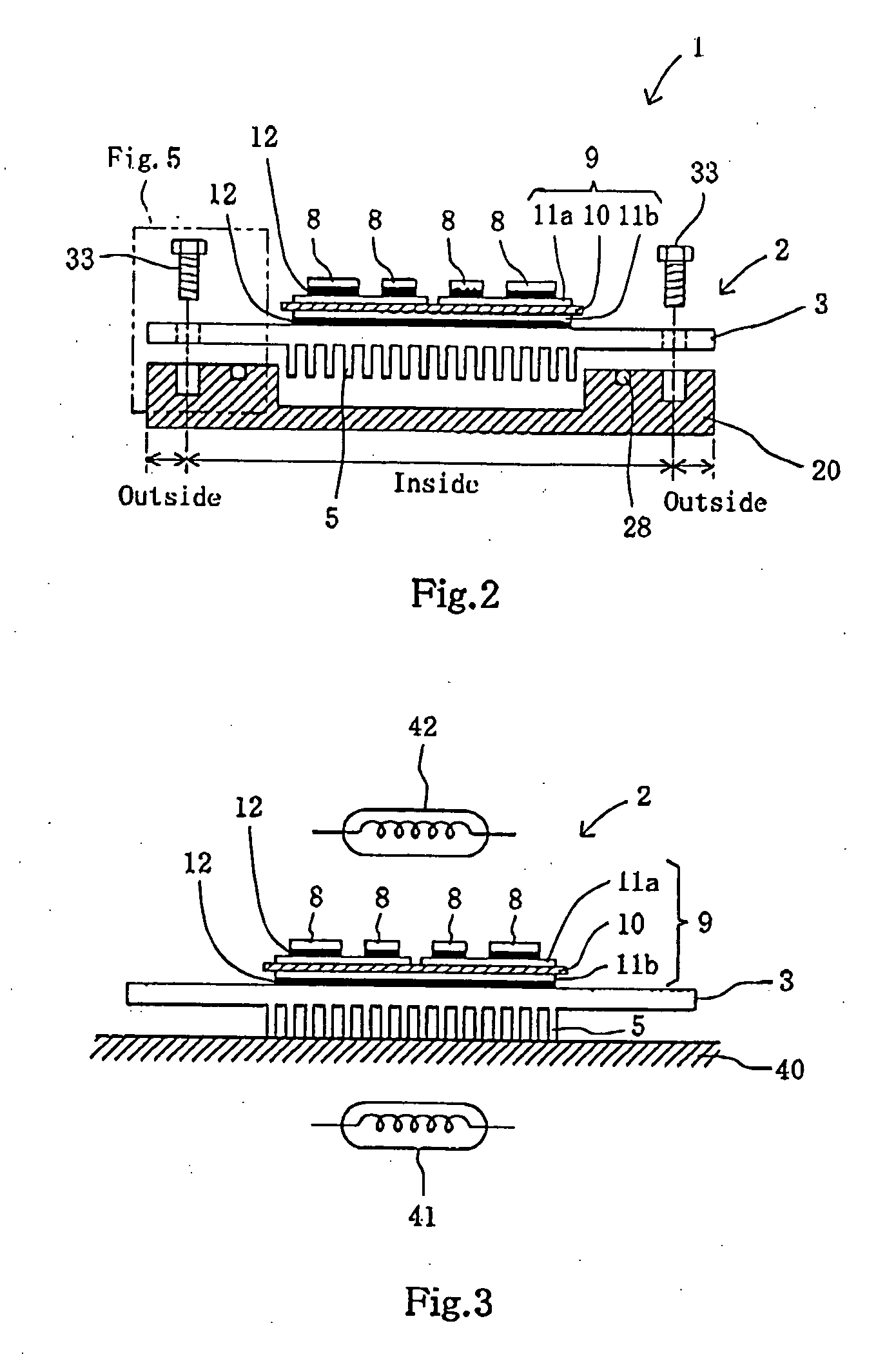
[0060]FIGS. 6A and 6B are respectively a perspective view of a 600V / 600A class direct cooling-type power semiconductor module 2 seen from the top surface side, and a perspective view thereof seen from the bottom surface side. In FIG. 6A, the finned base plate 3 has three insulated substrates 9 disposed on the top surface. In the present embodiment, the insulated substrates 9 are each made up of aluminum nitride, and they are all configured in the same manner. The insulated substrates 9 constitute upper and lower arms of a phase U inverter, a phase V inverter, and a phase W inverter, respectively.

[0061]In the present embodiment, the finned base plate 3 has a size of 10 cm×21 cm. In addition, the finned base plate 3 is 11 mm thick, including the planer base plate 4 located on the top surface side, which is 3 mm thick. The material of the finned base plate 3 is an Al—SiC composite material, and each surface thereof is plated with Ni. The finned base plate 3 is made by impregnating a mo...

second embodiment

[0074]The radiation fins 5 can be formed into another shape. For example, the finned base plate 3 according to a second embodiment shown in FIG. 10 includes wavy radiation fins 5 having a large contact area with the cooling medium and a high thermal conduction coefficient. The wavy radiation fins 5 are disposed along the flowing direction of the cooling medium. In addition, the wavy radiation fins 5 are disposed so as to converge immediately below the power semiconductor elements, and therefore it is possible to efficiently radiate heat while minimizing, insofar as possible, the pressure loss of the cooling medium flow. Note that the radiation fins 5 can be provided in the form of pin-fin arrays having a high thermal conduction coefficient and a superior radiation performance.

third embodiment

[0075]A power semiconductor device 1 according to a third embodiment shown in FIG. 11 can be integrated with a drive motor for hybrid or electric vehicles by applying a planar ring-like finned base plate 3. A plurality of radiation fins 51 are concentrically disposed about the center axis of the ring, as shown in FIG. 11. With the configuration shown in FIG. 11, the end wall of a housing 23 for the drive motor that includes the intake port 21 and the discharge port 22 can be used in place of the cooling jacket 20 to form the flow passage for the cooling medium, thereby making it possible to achieve a reduction in size and weight as well as a reduction in cost. In addition, an inverter device can be disposed close to the drive motor to be driven by the inverter device, so that circuit connection wiring can be shortened, thereby reducing power loss via the wiring.

[0076]Furthermore, the power semiconductor device 1 according to the present embodiment has a hollowed portion that can be ...


PUM


Abstract

A power semiconductor module according to the present invention includes: a planar base plate having a plurality of insulated substrates soldered on the top surface, the insulated substrates each having power semiconductor elements to be cooled mounted thereon; a plurality of radiation fins projecting from the bottom surface side of the base plate; and a peripheral wall projecting from the bottom surface side of the base plate so as to surround the radiation fins, the projecting length of the radiation fins is less than or equal to that of the peripheral wall, and the peripheral wall has end surfaces present in the same plane. In addition, a power semiconductor device having the power semiconductor module mounted therein includes: at least one reinforcing plate disposed on the top surface side of the base plate via a first buffering member; and a cooling jacket fixed to the bottom surface side of the base plate via a second buffering member with a plurality of tightening fixtures passing through the reinforcing plate and the base plate, the cooling jacket having a flow passage for a cooling medium formed to intervene in a position with respect to the base plate, and the first buffering member and the second buffering member are respectively disposed at least inside and outside with respect to the tightening fixtures.

Description

CROSS REFERENCE TO RELATED APPLICATION[0001]The disclosure of Japanese Patent Applications No. 2007-092777 filed Mar. 30, 2007 and No. 2007-159783 filed Jun. 18, 2007 including specification, drawings and claims is incorporated herein by reference in its entirety.BACKGROUND OF THE INVENTION[0002]1. Field of the Invention[0003]The present invention relates to power semiconductor modules in which insulated substrates provided with power semiconductor elements made up of silicon (Si) or silicon carbide (SiC), such as IGBTs (insulated gate bipolar transistors) and MOS FETs, are mounted on a base plate, which is directly cooled by a cooling medium, and the present invention also relates to power semiconductor devices having such a module mounted therein.[0004]2. Description of the Background Art[0005]Typically, hybrid vehicles or electric vehicles use electric power conversion equipment (hereinafter, an “inverter device”) for driving a large capacity drive motor. A power semiconductor mo...

Claims


Application Information

Patent Timeline
IPC IPC(8): H01L23/467
CPCH01L23/367H01L23/473H01L25/072F28F3/12H01L2924/13091H01L2924/19107H01L2924/13055H01L2924/1305H01L2224/32225H01L2924/00
Inventor NAKANISHI, RAITAKAWAMURA, TOSHIAKI
Owner NICHICON CORP
Why Eureka
Try Eureka