Electron beam apparatus

a technology of electric beam and beam tube, which is applied in the direction of electric discharge tube/lamp manufacture, discharge tube luminescnet screen, instruments, etc., and can solve the problem of new discharg

Inactive Publication Date: 2008-10-02
CANON KK
View PDF13 Cites 10 Cited by
  • Summary
  • Abstract
  • Description
  • Claims
  • Application Information

AI Technical Summary

Benefits of technology

[0096]Subsequently, discharge experiments in which the device discharge is artificially induced by applying an overvoltage to the electron-emitting devices are executed in order to confirm the effects of the invention. First, at the center of the panel, the electron-emitting devices other than the pixel at a proper address (X, Y) in the position away from the spacers and its three peripheral pixels are removed. This is because in the discharge experiments, if the electron-emitting devices are connected onto the wiring to be driven, when the voltage is applied, the current according to the device characteristics is added to the discharge current. As a removing method of the electron-emitting devices, such a device removal is realized by irradiating a YAG laser from the back surface of the rear plate to the device film 7. Since the device film 7 is a very thin film, it can be removed even at a low power.
[0097]Subsequently, a voltage of 1 to 10 kV is applied to the anode electrode of the face plate, a voltage of −10 to 20 V is applied as a scan signal, and a voltage of +10 to 20 V is applied as an information signal, respectively. At the same time, the voltage on the voltage applied line and a current waveform are monitored by using a voltage probe and a current probe.
[0098]In the example, since a resistance of a voltage applying path on the scan signal side is smaller than that on the information signal side, most of the discharge current flows to the scan signal wiring. In an electric circuit manner, a shunt ratio of (the scan signal side:the information signal side) is equal to (10:1). However, as illustrated in FIG. 3, since the cathode spot 21 moves on the scan signal device electrode 1 and the device film 7 is destroyed to thereby raise the resistance, the current flowing to the information signal side may be regarded to be almost zero. Actually, the discharge current from the information signal wiring 4 is equal to 20 mA or less.
[0099]FIGS. 11A to 11C illustrate schematic diagrams of waveforms of the discharge current output from the scan signal wiring 6 in the embodiment. In the embodiment, values of times T0 to T5 and currents A1 to A3 in FIGS. 11A to 11C are as follows.
[0109]Current values of A1 to A3 are adjusted based on a value of the voltage applied to the face plate. In the case of the current value of A1, the discharge is finished for a time T1 in Examples 1 to 3. In the case of the current value of A2, the discharge is finished for a time T3 in Examples 1 and 2. In the case of the current value of A3, the discharge is finished for a time T5 in

Problems solved by technology

However, in those constructions, if the overcurrent is caused by a discharge current, there is a case where a new discharge further occurs and continues in the fusing portion.

Method used


Image

  • Electron beam apparatus
  • Electron beam apparatus
  • Electron beam apparatus

Examples


example 1

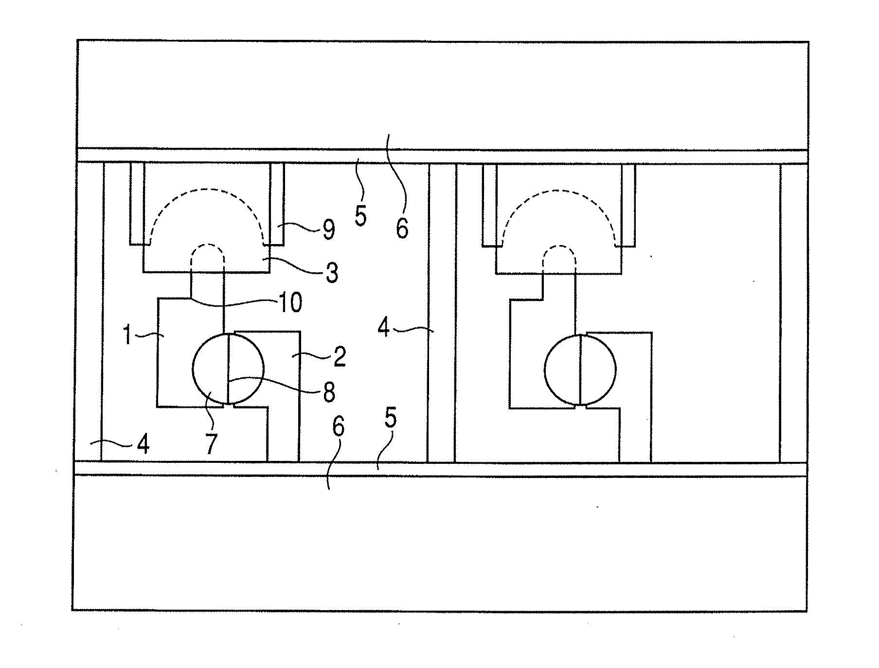
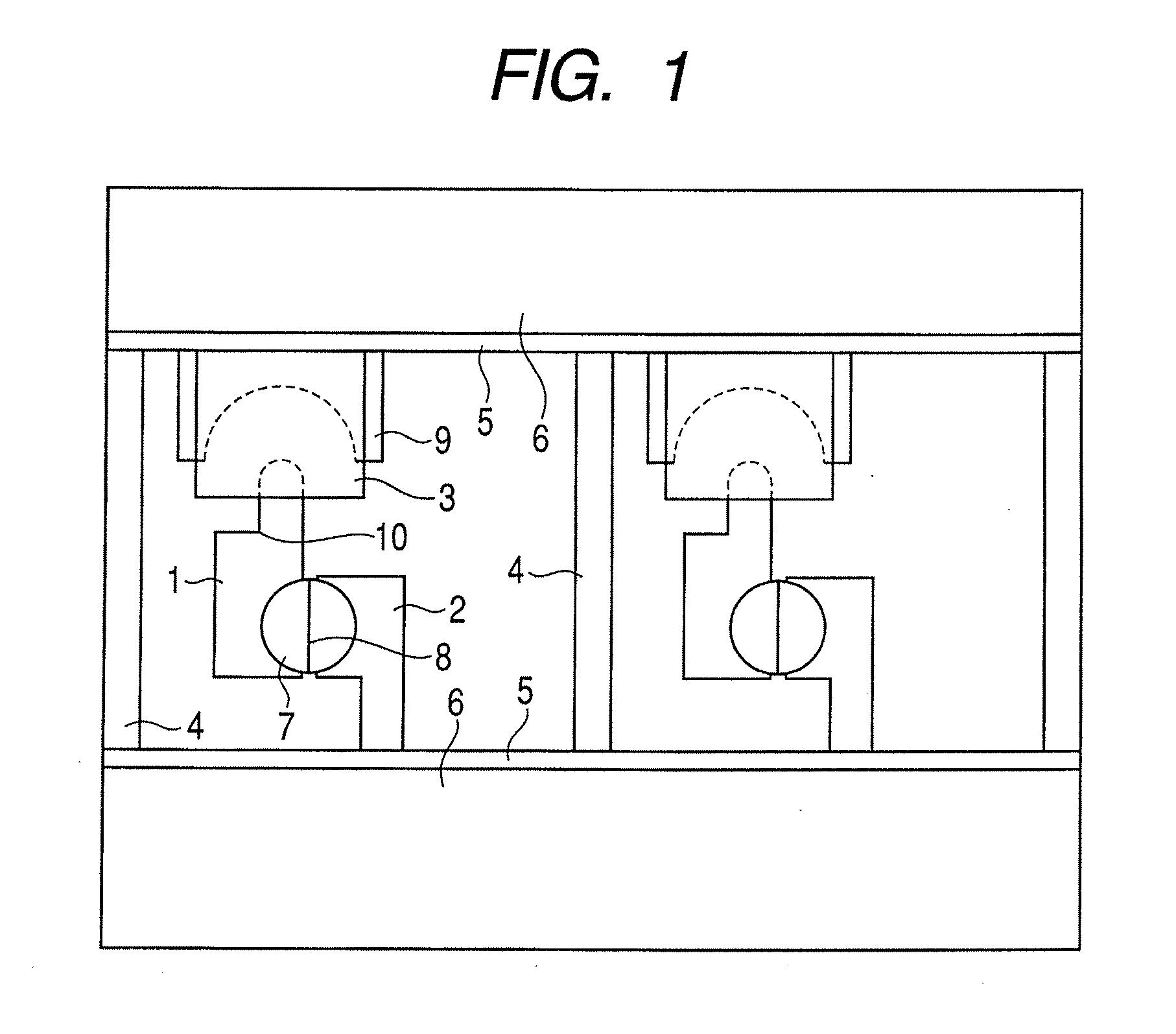
[0071]The rear plate illustrated in FIG. 1 is manufactured according to the steps illustrated in FIG. 2. In this example, glass having a thickness of 2.8 mm of PD-200 (made by Asahi Glass Co., Ltd.) in which an amount of alkali component is small is used as a substrate and, further, the glass substrate is coated with an SiO2 film having a thickness of 200 nm as a sodium block layer.

[0072]

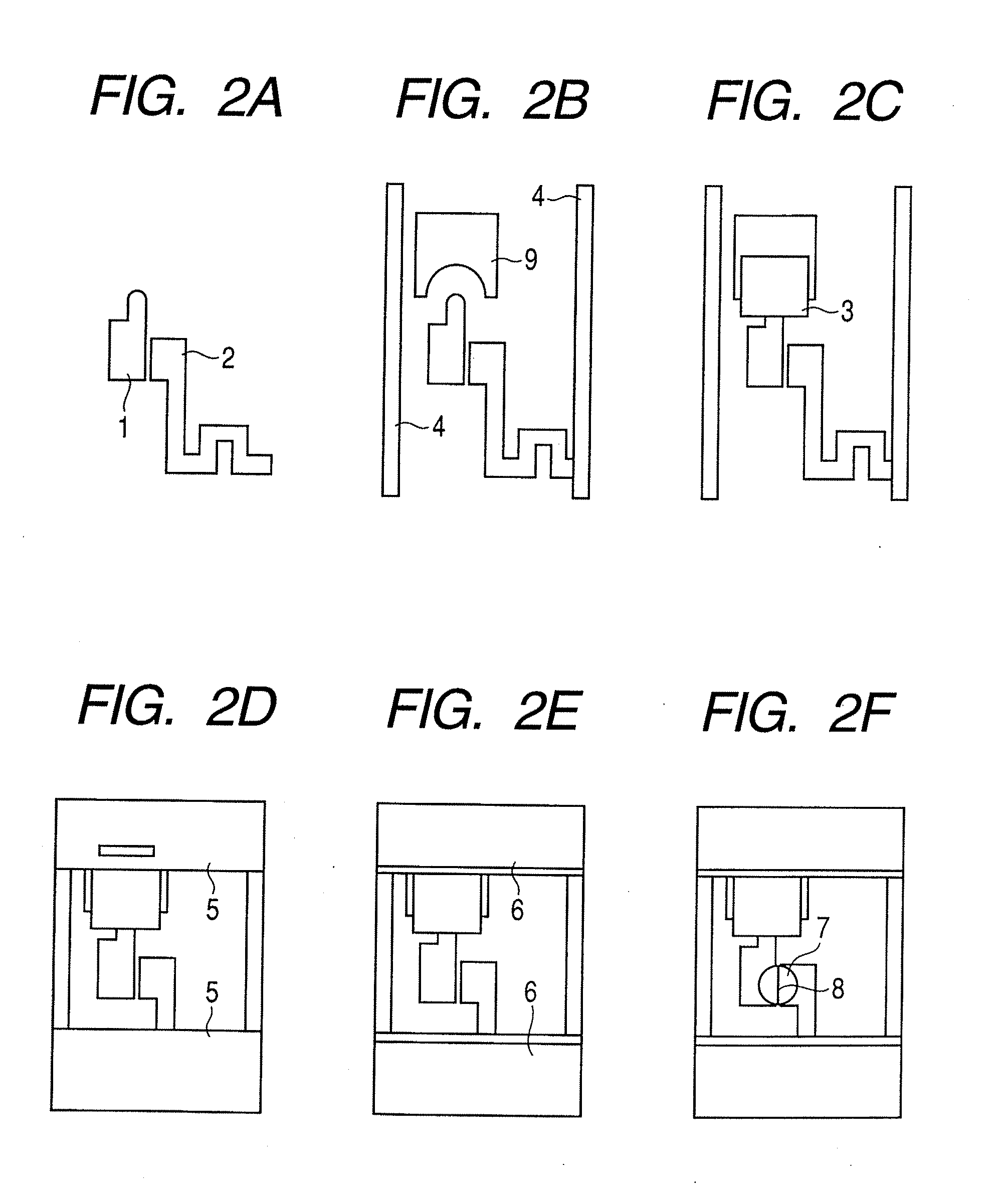
[0073]A Ti / Pt film having a thickness of 5 / 20 nm is formed onto the glass substrate by a sputtering method. After that, the whole surface is coated with a photoresist. Subsequently, a patterning is performed by a series of photolithography technique such as exposure, development, and etching, thereby forming the scan signal device electrode 1 and the information signal device electrode 2 (FIG. 2A). The information signal device electrode 2 is formed in a zigzag shape so as to have a high resistance. An electrical resistivity of each of the device electrodes 1 and 2 is equal to 0.25×10⁻⁶ [Ωm]. In the...

example 2

[0089]A rear plate with a construction illustrated in FIG. 7 is manufactured. Since its manufacturing steps are similar to those in FIG. 2, their description is omitted here.

[0090]A thickness of extension wiring 9 is set to about 10 μm, its width is set to 80 μm, and its length is set to 130 μm. A thickness of additional electrode 3 is set to about 1 μm, its width is set to 60 μm, and its length is set to 30 μm.

[0091]In the scan signal device electrode 1, a width of electrode connected to the device film 7 is set to 20 μm and a width of electrode connected to the additional electrode 3 is set to 10 μm, and the distance L1 between the position 26 which is electrically closest to the scan signal wiring 6 and the high temperature portion 23 is set to 15 μm.

example 3

[0092]The rear plate is manufactured in a manner similar to Example 1 except that the device electrodes 1 and 2 and the extension wiring 9 are simultaneously made of the same material.


PUM


Abstract

The invention provides an electron beam apparatus having: a rear plate having a plurality of electron-emitting devices each provided with a device electrode, and a plurality of wirings connected to the device electrodes; and a face plate being provided with an anode electrode, and being arranged in opposition to the rear plate so as to be irradiated with an electron emitted from the electron-emitting device, wherein the device electrode is electrically connected to the wiring through an additional electrode, and the additional electrode is formed from an electroconductive material of which phase transition from a solid phase directly into a vapor phase is caused at a temperature not lower than a melting point of the device electrode within an evacuated atmosphere.

Description

BACKGROUND OF THE INVENTION[0001]1. Field of the Invention[0002]The present invention relates to an electron beam apparatus which uses electron-emitting devices and which is applied to a flat panel type image display apparatus (flat panel display) and, more particularly, to an electron beam apparatus having a feature in an electrode construction of a rear plate.[0003]2. Description of the Related Art[0004]Hitherto, an image forming apparatus can be mentioned as a using form of electron-emitting devices. For example, there is a flat panel type electron beam display panel in which an electron source substrate (rear plate) formed with a number of cold cathode electron-emitting devices and an opposite substrate (face plate) having anode electrodes each for accelerating an electron emitted from the electron-emitting device and a light-emitting member are arranged in parallel so as to face each other and the inside of the display panel has been evacuated in vacuum. According to the flat p...

Claims


Application Information

Patent Timeline
Patent Type & Authority Applications(United States)
IPC IPC(8): H01J29/02
CPCH01J1/316H01J29/04H01J31/127H01J2201/3165H01J2329/0489
Inventor IBA, JUNAZUMA, HISANOBU
Owner CANON KK
Why Eureka
Try Eureka