Nanodot electroluminescent diode of tandem structure and method for fabricating the same

a tandem structure and diode technology, applied in the direction of discharge tube luminescnet screens, discharge tube/lamp details, electric discharge lamps, etc., can solve the problems of efficiency, luminance, and persistence of mixed color arrangement, and achieve high efficiency, stability, and multi-color effects

Inactive Publication Date: 2008-10-02
SAMSUNG ELECTRONICS CO LTD
View PDF0 Cites 51 Cited by
  • Summary
  • Abstract
  • Description
  • Claims
  • Application Information

AI Technical Summary

Benefits of technology

[0008]Disclosed is a multiple nanodot electroluminescent diode, and a method for fabricating the multiple nanodot electroluminescent diode, in which a plurality of unit cells, each of which includes a quantum dot electroluminescent layer and an organic layer and / or an inorganic layer, are interposed between a lower electrode and an upper electrode to obtain high efficiency, stability, multi-colors, and high luminance.

Problems solved by technology

Despite effort on application of quantum dots as a light-emitting layer in LEDs, problems with efficiency, luminance, and arrangement of mixed colors persist.

Method used


Image

  • Nanodot electroluminescent diode of tandem structure and method for fabricating the same
  • Nanodot electroluminescent diode of tandem structure and method for fabricating the same
  • Nanodot electroluminescent diode of tandem structure and method for fabricating the same

Examples


example 1

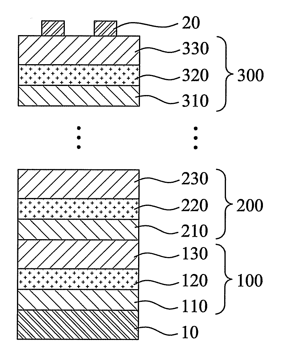
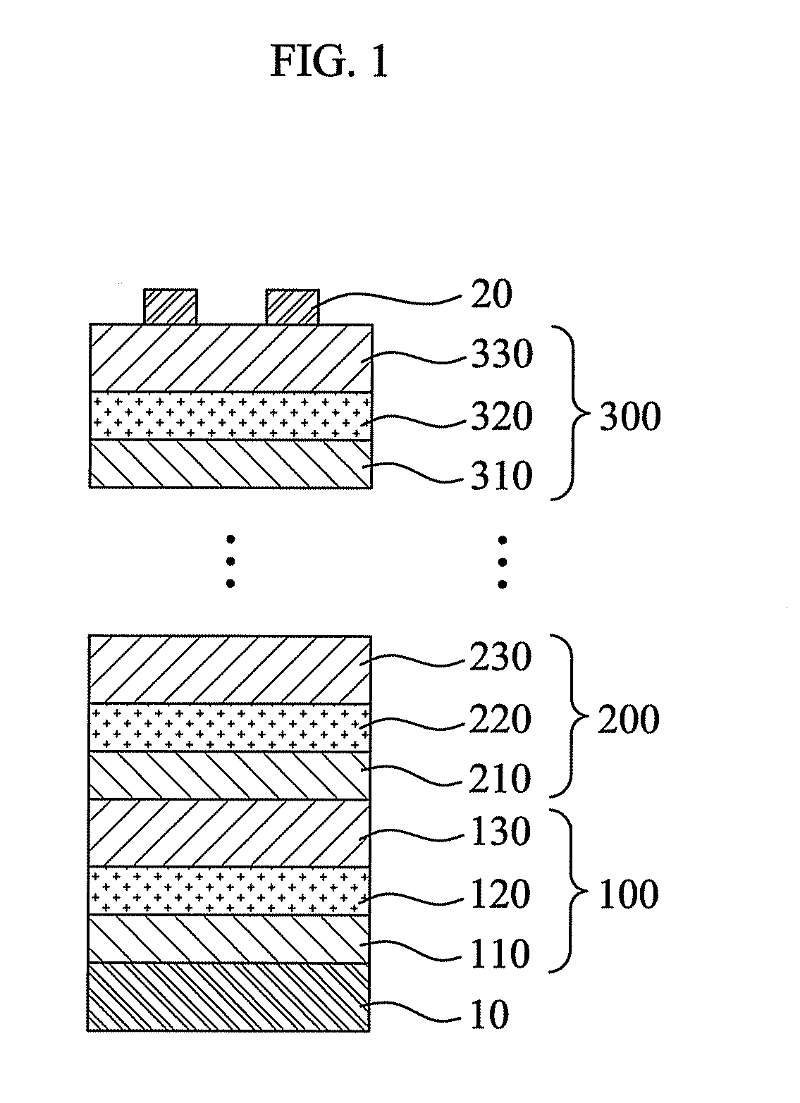
[0049]A wafer, patterned with ITO, was washed sequentially with solvent such as a neutral detergent, deionized water, water, isopropylalcohol, or the like, or a combination of at least one of the foregoing solvents. The patterned wafer was then treated with UV-ozone. A PEDOT solution was then spin-coated on to the wafer for 30 seconds at 2000 revolutions per minute (rpm) to obtain a thin film having a thickness of about 50 nanometers (nm). Next, a 0.5 weight percent solution of PVK (poly(vinylcarbazole)) in chlorobenzene was spin-coated on to the wafer for 30 seconds at 2000 rpm to obtain a thin film having a thickness of 20 nm. The PVK coated wafer was then dried for 20 minutes in a vacuum. CdSe / ZnS core / shell nanocrystal (Evidot 630 nm absorbance, used as received commercially from Evident Technology, product name: Evidot Red(CdSe / ZnS) was spin-coated on the PVK film for 30 seconds at 2000 rpm and dried for 5 minutes at 50° C. to provide a quantum electroluminescent layer. The qua...

example 2

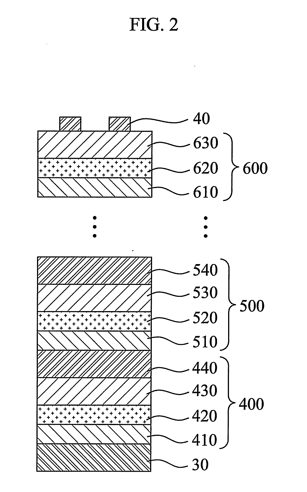
[0055]In Example 2, a diode was fabricated using two types of quantum dot electroluminescent layers, one red and one green. The diode according to Example 2 was fabricated by the same method as Example 1 except that in the second unit cell a green luminescing CdSe / ZnS core / shell nanocrystal (Evidot 630 nm absorbance, used as received commercially from Evident Technology, product name: Evidot green (CdSe / ZnS) at 0.3 weight percent (wt %) was used for the quantum dot electroluminescent layer.

[0056]FIG. 7 illustrates the electroluminescence of a comparative example and is an electroluminescence (EL) spectrum illustrating a nanodot electroluminescent diode where a unit cell including a green quantum dot electroluminescent layer is interposed between a lower electrode and an upper electrode.

[0057]FIG. 8 is an EL spectrum illustrating a multiple nanodot electroluminescent diode where a unit cell including a red quantum dot electroluminescent layer and a unit cell including a green quantum...


PUM


Abstract

A nanodot electroluminescent diode is disclosed. The nanodot electroluminescent diode comprises a lower electrode, an upper electrode, and unit cells interposed between the electrodes, wherein the unit cells comprise a quantum dot electroluminescent layer and also include an organic layer and/or an inorganic layer in addition to the quantum dot electroluminescent layer. The disclosed nanodot electroluminescent diode provides high efficiency, stability, and high luminance, and mixed colors, multi-colors, full color, and white electroluminescence can be obtained.

Description

CROSS-REFERENCE TO RELATED APPLICATIONS[0001]This application claims priority to Korean Patent Application No. 10-2007-0006725, filed on Jan. 22, 2007, and all the benefits accruing therefrom under 35 U.S.C. § 119, the contents of which are herein incorporated by reference in its entirety.BACKGROUND OF THE INVENTION[0002]1. Field of the Invention[0003]The disclosed embodiments relate to a nanodot electroluminescent diode and a method for fabricating the nanodot electroluminescent diode to obtain high efficiency, stability, multiple colors, and high luminance.[0004]2. Description of the Related Art[0005]A quantum dot is a nanocrystal of a metal or a semiconductor having a size smaller than a Bohr exciton radius, i.e., several nanometers. Although a large number of electrons can exist within a quantum dot, the number of free electrons is finite, thus the number of free electrons can be in an amount of 1 to about 100. In this case, since the electron energy levels are discontinuous, el...

Claims


Application Information

Patent Timeline
Patent Type & Authority Applications(United States)
IPC IPC(8): H01J1/62H01L33/06H01L33/08H01L33/28H01L33/34
CPCB82Y20/00B82Y30/00H01L27/3209H01L51/5012H01L51/5278H05B33/14H10K59/32H10K50/11H10K50/19H05B33/02
Inventor CHO, KYUNG SANGCHOI, BYOUNG LYONGKWON, SOON JAE
Owner SAMSUNG ELECTRONICS CO LTD
Why Eureka
Try Eureka