Method for incorporating transistor snap-back protection in a level shifter circuit

a level shifter circuit and transistor technology, applied in logic circuits, pulse automatic control, pulse techniques, etc., can solve the problems of significant reliability concerns, limiting the operating voltage achievable, and the problem of more problems with snapping back problems in nmos devices than in pmos devices

Active Publication Date: 2008-10-02
SANDISK TECH LLC
View PDF34 Cites 20 Cited by
  • Summary
  • Abstract
  • Description
  • Claims
  • Application Information

AI Technical Summary

Benefits of technology

[0018]Improved level shift circuits are disclosed for level shifting an input signal corresponding to a first voltage domain, to generate an output signal or a pair of complementary output signals corresponding to a second higher-voltage domain. Snap-back sensitive devices in a discharge circuit for a high voltage output node are protected by a voltage shifter circuit in series with the sensitive devices, to limit the voltage across a sensitive device irrespective of the loading on the output node, and even for a high capacitance output node at the highest output voltage. This may be achieved without requiring precise transistor sizing, as a function of the output loading, to carefully control how quickly certain transistors are turned fully on. The voltage shifter circuit is then bypassed to provide for an output low level that fully reaches the lower power supply rail.

Problems solved by technology

However, when such a transistor is conducting, the maximum voltage that may be safely applied from drain to source terminals is frequently a lower voltage than the breakdown voltage.
Snap back concerns frequently limit the operating voltage achievable in a level shifting circuit, and may pose significant reliability concerns in such level shifting circuits.
Snap back problems are more problematic in NMOS devices than in PMOS devices, because of the greater susceptibility of electrons being trapped in oxides and surface traps than the susceptibility for holes being trapped.
Snap back can cause catastrophic failure of a device, and hence the failure of a circuit incorporating such a device.
Consequently, snap back problems are more likely to arise in sub-circuits used to discharge a high voltage node, such as an output node of a level shifter circuit.
However, a suitable high voltage device for 10 volt operation likely requires a threshold voltage high enough (e.g., VT=600-1200 mV) that a VDD level signal on its gate (e.g., as low as 1.2 volts) would barely turn on such a device, if at all.
The weakened drive strength in both the charging (i.e., pull-up) path and the discharging (i.e., pull-down) path increases the delay through such a level shifter circuit, and thus reduces circuit performance.
As a result, no standard-sized level shifter circuit may be used with varying output capacitive loading without risking the reliability of the level shifter circuit.
Considerable efforts have been applied in the art to design around such snap back concerns, which sometimes results in circuits having unusually high complexity to accomplish what might seem like a simple logic structure.

Method used


Image

  • Method for incorporating transistor snap-back protection in a level shifter circuit
  • Method for incorporating transistor snap-back protection in a level shifter circuit
  • Method for incorporating transistor snap-back protection in a level shifter circuit

Examples


Embodiment Construction

)

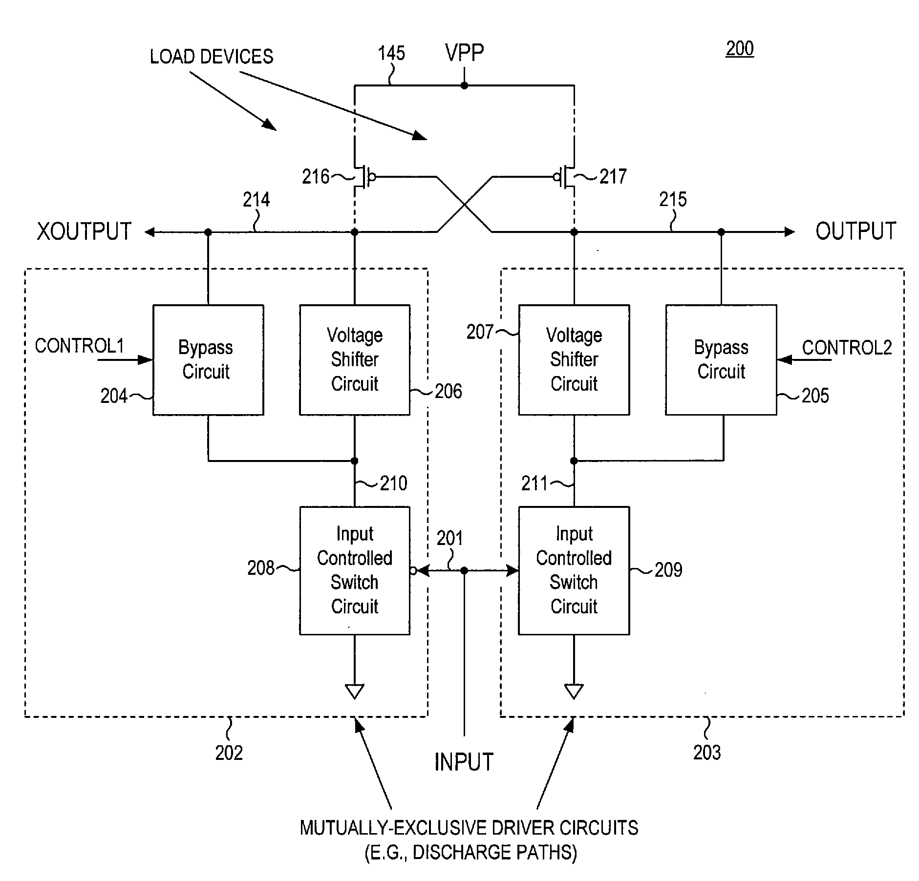
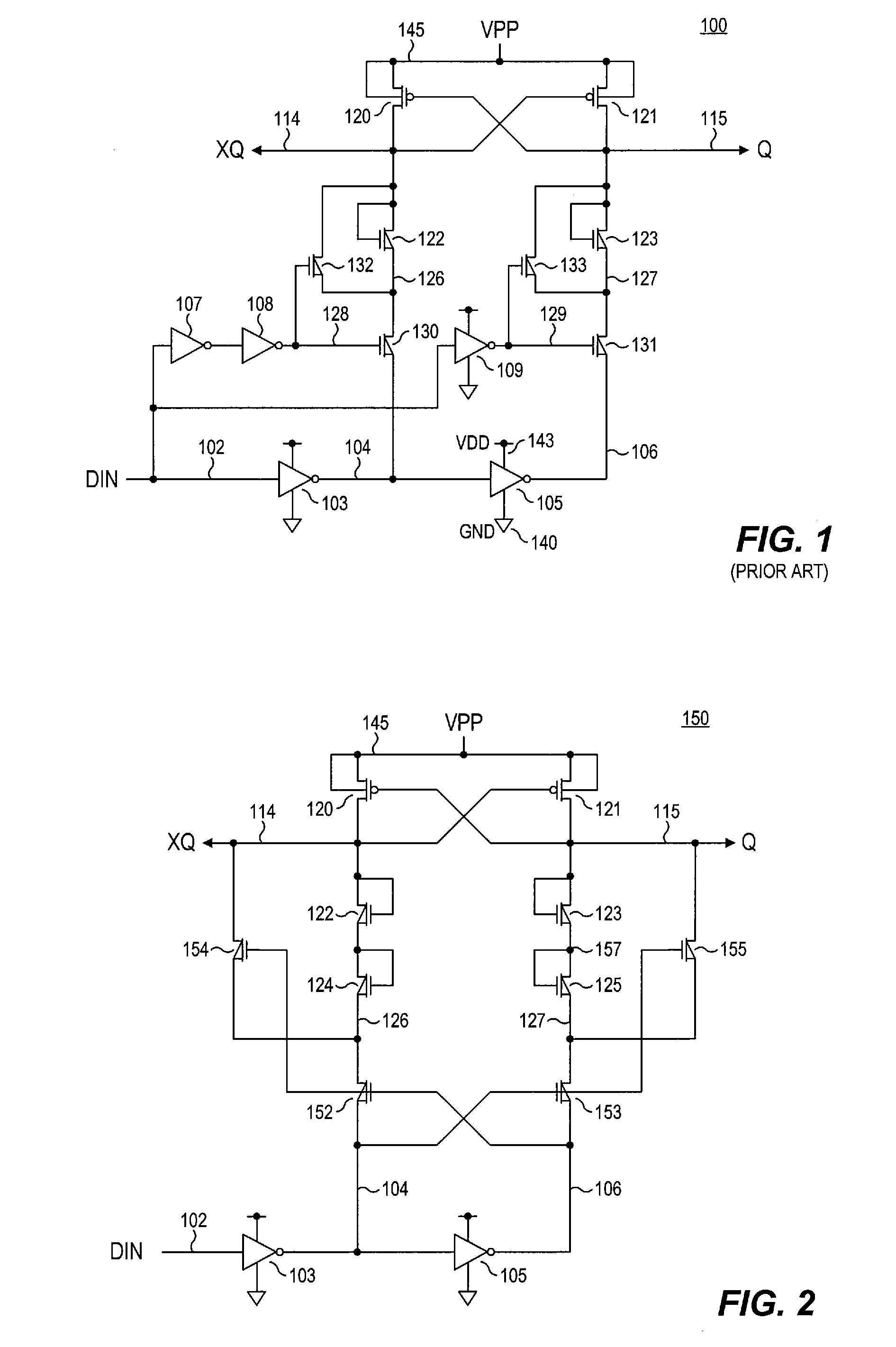
[0031]Referring now to FIG. 2, a level shifting circuit is shown that does not require intentionally weakened pull down paths, and yet is protected from snapback effects independent of output load. As before, a logic signal DIN is conveyed on node 102, and is inverted by low-voltage inverter 103 to generate the VDD-level control signal on node 104, which is inverted by low-voltage inverter 105 to generate the VDD-level control signal on node 106. The inverters 103, 105 may be viewed as belonging to the VDD voltage domain (i.e., the low voltage domain), and the input signal DIN conveyed on node 102 and the control signals conveyed on nodes 104, 106 may be viewed as VDD domain (i.e., low-voltage domain) signals having high and low levels respectively corresponding to VDD and ground.

[0032]The complementary XQ, Q output nodes 114, 115 are coupled to VPP by cross-coupled PMOS transistors 120, 121, and are coupled to ground by generally matching discharge circuits. The XQ output node 114...


PUM


Abstract

Level shift circuits are disclosed for level shifting an input signal corresponding to a first voltage domain, to generate a pair of complementary output signals corresponding to a second, higher-voltage domain. Snap-back sensitive devices in a discharge circuit for a high voltage output node are protected, irrespective of the loading on the output node, and without requiring precise transistor sizing as a function of the output loading. The snap-back sensitive devices are protected by a voltage shifter circuit in series with the sensitive devices, to limit the voltage across the sensitive devices, even for a high capacitance output node at its highest output voltage. The voltage shifter circuit is then bypassed to provide for an output low level that fully reaches the lower power supply rail.

Description

CROSS-REFERENCE TO RELATED APPLICATION(S)[0001]This application is related to the following co-pending U.S. Application(s), each of which is incorporated by reference herein in its entirety:[0002]U.S. application Ser. No. ______ (Attorney Docket 023-0061) entitled “Level Shifter Circuit Incorporating Transistor Snap-Back Protection” by Tyler J. Thorp and Luca G. Fasoli, filed on even date herewith.BACKGROUND[0003]1. Field of the Invention[0004]The present invention relates to level shifting circuits for generating a high voltage domain output signal responsive to a low voltage domain input signal.[0005]2. Description of the Related Art[0006]Level shifting circuits are commonly used to convert a signal from a low voltage domain to a high voltage domain. For example, a logic signal may be generated by circuitry which is powered by a low-voltage power supply voltage, such as VDD (e.g., 1.5 volts), and thus have output levels generally corresponding to VDD and ground. However many circu...

Claims


Application Information

Patent Timeline
Patent Type & Authority Applications(United States)
IPC IPC(8): H03L5/00
CPCH03K3/356182
Inventor THORP, TYLER J.FASOLI, LUCA G.
Owner SANDISK TECH LLC
Why Eureka
Try Eureka