Photoelectric conversion device and fabrication method thereof

a conversion device and photoelectric technology, applied in the direction of semiconductor/solid-state device manufacturing, semiconductor devices, electrical devices, etc., can solve the problems of low photoelectric conversion efficiency, high fabrication cost of photovoltaic power generation, and restricted use, and achieve excellent band gap energy, high photoelectric conversion efficiency, and excellent physical and mechanical properties of diamond

Inactive Publication Date: 2008-10-09
LG ELECTRONICS INC
View PDF2 Cites 11 Cited by
  • Summary
  • Abstract
  • Description
  • Claims
  • Application Information

AI Technical Summary

Benefits of technology

[0049]The DLC film can be physically controlled so that the excellent physical and mechanical properties of diamond are well harmonized with the excellent electrical properties of graphite by controlling a coupling amount of diamond and graphite.
[0050]The method according to one embodiment of the present inve

Problems solved by technology

A silicon single crystal solar cell currently widely commercialized for photovoltaic power generation is high in fabricating costs due to use of an expensive wafer, as such its use is restricted.
It has a disadvantage of relatively low photoelectric conversion efficiency as compared to a crystalline sili

Method used


Image

  • Photoelectric conversion device and fabrication method thereof
  • Photoelectric conversion device and fabrication method thereof
  • Photoelectric conversion device and fabrication method thereof

Examples


Embodiment Construction

[0058]Embodiments of the present invention will now be described hereafter with reference to the attached drawings. Reference numerals added to construction elements of each drawings use the same numerals within the range of the same construction elements, even though they are indicated in the other drawings, and the detailed description about well-known functions and structures, which are outside the subject matter of the present invention will be omitted.

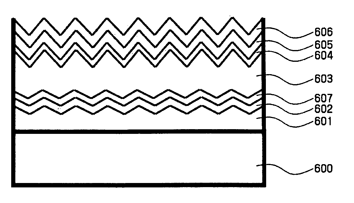
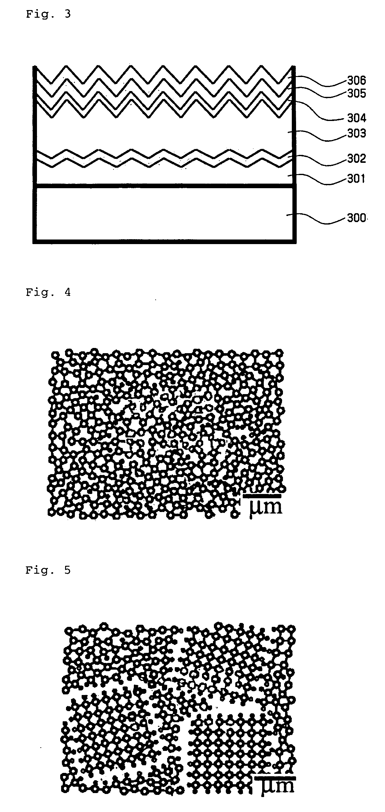
[0059]FIG. 3 is a cross-sectional view schematically showing a stacked structure of a photoelectric conversion device according to one embodiment of the present invention.

[0060]Referring to FIG. 3, there is shown a photoelectric conversion device wherein a p-type semiconductor layer 302 is formed on a transparent conductive oxide layer 301 stacked on a substrate 300.

[0061]The p-type semiconductor layer 302 is made of hydrogenated amorphous carbon (a-C:H) film doped with boron (B) or diamond like carbon (DLC) film doped with boron ...


PUM


Abstract

A photoelectric conversion device includes at least one p-type semiconductor layer made of amorphous like hydrogenated carbon film or diamond like carbon (DLC) film doped with acceptor impurities such as boron (B). In a solar cell having a photoelectric conversion region, hydrogenated carbon is used as substances forming a p-type semiconductor layer, making it possible to provide a solar cell with high photoelectric conversion efficiency.

Description

BACKGROUND OF THE INVENTION[0001]This application claims priority to Korean Patent Application No. 10-2007-0034787, filed on Apr. 9, 2007, in the Korean Intellectual Property Office, the entire contents of which are hereby incorporated by reference.[0002]1. Field of the Invention[0003]The present invention relates to a photoelectric conversion device and a fabrication method thereof, and more specifically to a photoelectric conversion device and a fabrication method thereof using amorphous like hydrogenated carbon film or diamond like carbon (DLC) film doped with acceptor impurities such as boron (B) as substances forming a p-type semiconductor layer, in a solar cell having a photoelectric converting region.[0004]2. Description of the Prior Art[0005]A study on photovoltaic power generation as a next-generation clean energy source has actively been progressed since it does not cause environmental disruption by using new renewable energy and can obtain energy anywhere.[0006]A silicon ...

Claims


Application Information

Patent Timeline
IPC IPC(8): H01L31/0264H01L31/0376H01L31/18
CPCH01L31/028H01L31/0745H01L31/075Y02E10/548Y02E10/547H01L31/0445H01L31/18
Inventor KIM, HWA NYEONKIM, BUM SUNGLEE, HAE SEOKYUN, JUNG HEUMLEE, HEON MIN
Owner LG ELECTRONICS INC
Why Eureka
Try Eureka