Transistor Based on Resonant Tunneling Effect of Double Barrier Tunneling Junctions

a tunneling junction and transistor technology, applied in the field of solid-state switching and amplifying devices, can solve the problems of difficult to fabricate perfect double-barrier tunneling junctions, lack of control, etc., and achieve the effects of low leakage current, high collector current, and large outpu

Inactive Publication Date: 2008-10-09
INST OF PHYSICS - CHINESE ACAD OF SCI
View PDF4 Cites 27 Cited by
  • Summary
  • Abstract
  • Description
  • Claims
  • Application Information

AI Technical Summary

Benefits of technology

[0033]The transistor device based on double barrier tunneling junctions of the present invention overcomes the Schottky potential produced between a base and a collector because a double-barrier structure is used. The transistor has comparatively low leakage current and comparatively high collector current. At the same time, devices based on this kind of structures have certain current or vo

Problems solved by technology

However, this kind of transistors has following shortcomings due to the Schottky potential produced between base and collector: □ lacking of the control of base-collector potential; □ high leakage current under low emitter-base voltage.
However, because there were s

Method used


Image

  • Transistor Based on Resonant Tunneling Effect of Double Barrier Tunneling Junctions
  • Transistor Based on Resonant Tunneling Effect of Double Barrier Tunneling Junctions
  • Transistor Based on Resonant Tunneling Effect of Double Barrier Tunneling Junctions

Examples


embodiment 1

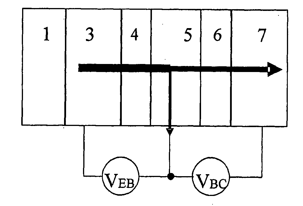
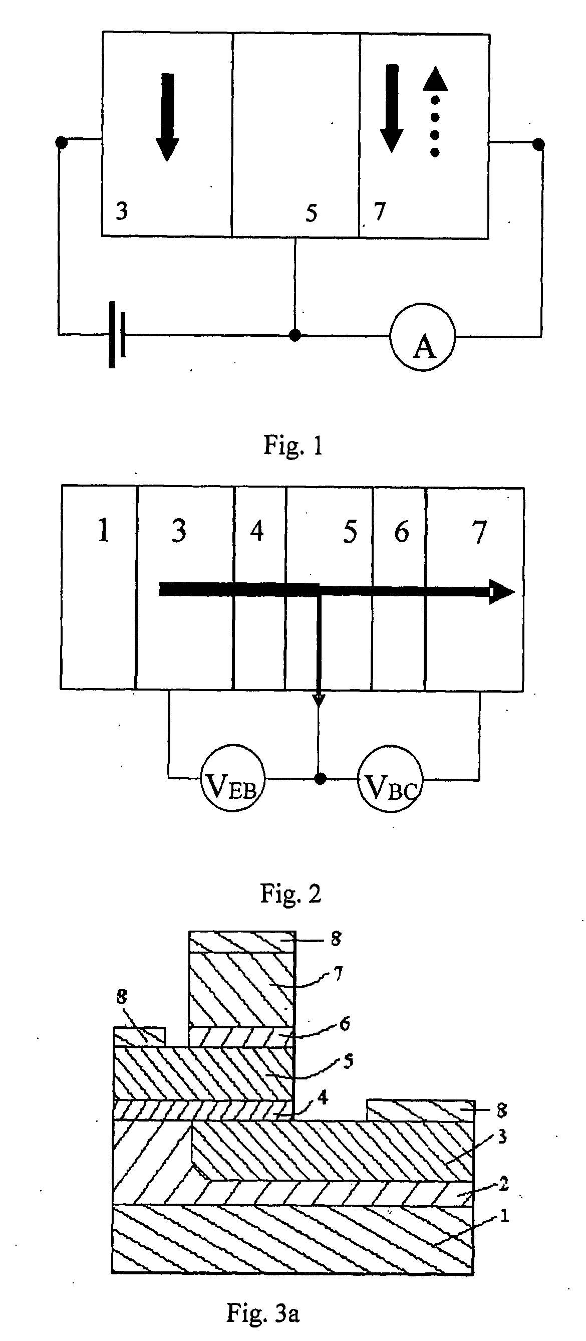
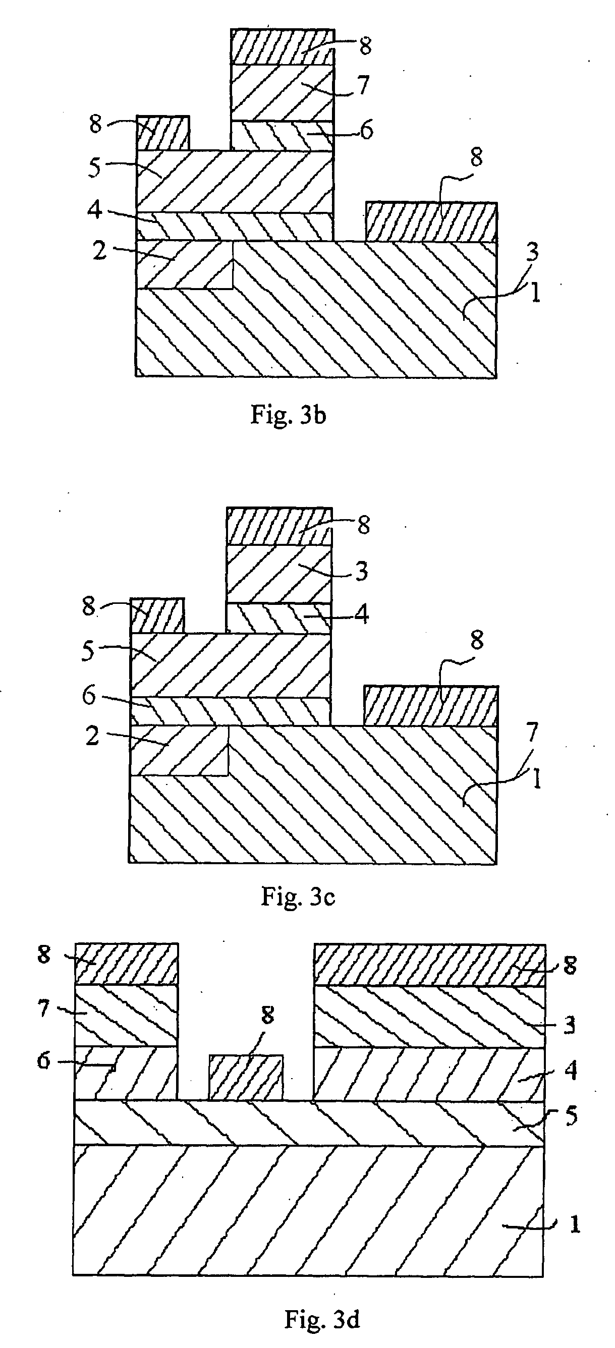
[0049]Referring to FIG. 3a, a spin transistor is provided based on the resonant tunneling effect of double barrier tunneling junctions of the present invention. In the spin transistor based on the resonant tunneling effect of double barrier tunneling junctions, a substrate 1 is made of a 0.4 mm-thick Si material, a 10 nm-thick insulating layer 2 made of SiO2 is formed on the Si substrate 1, an emitter 3 is formed on the insulating layer 2, comprising a 12 nm-thick antiferromagnetic layer of Ir—Mn and an 8 nm-thick layer of Fe, wherein the antiferromagnetic layer of Ir—Mn is used to fix the magnetization orientation of the emitter 3; a first tunneling barrier layer 4 made of Al2O3 material is formed on the emitter 3, being 1 nm in thickness. Furthermore, an 8 nm-thick base 5 is formed on the first tunneling barrier layer 4, being made of nonmagnetic metal Cu. An Al2O3 layer is formed on the base 5, acting as a second tunneling barrier layer 6 with 1.6 nm in thickness; a collector 7 m...

embodiment 2

[0051]Referring to FIG. 3a, a spin transistor is provided based on the resonant tunneling effect of double barrier tunneling junctions of the present invention. In the spin transistor based on the resonant tunneling effect of double barrier tunneling junctions, a substrate 1 is made of a 0.6 mm-thick Si material, a 100 nm-thick insulating layer 2 made of SiO2 is formed on Si substrate 1, an emitter 3 is formed on the insulating layer 2, comprising a 15 nm-thick antiferromagnetic layer of Fe—Mn and a 4 nm-thick layer of a semimetal material La0.7Sr0.3MnO3, wherein the magnetization orientation of the emitter 3 is fixed; a first tunneling barrier layer 4 made of SrTiO3 material is formed on the emitter 3, being 1.0 nm in thickness; furthermore, a 4 nm-thick base 5 is formed on the first tunneling barrier layer 4, being made of a layer of a nonmagnetic metal material Ru; a SrTiO3 layer is formed on the base 5, acting as a second tunneling barrier layer 6 with 1.3 nm in thickness; a col...

embodiment 3

[0054]Referring to FIG. 3a, a spin transistor is provided based on the resonant tunneling effect of double barrier tunneling junctions of the present invention.

[0055]In the spin transistor based on the resonant tunneling effect of double barrier tunneling junctions, a substrate 1 is made of a 0.6 mm-thick Si material, a 300 nm-thick insulating layer 2 made of SiO2 is formed on Si substrate 1, an emitter 3 is formed on the insulating layer 2, comprising a 4 nm-thick layer of a magnetic semiconductive material GaMnAs. The magnetization orientation of the emitter 3 is comparatively unbounded and can be changed by an external magnetic field; a first tunneling barrier layer 4 made of MgO material is formed on the emitter 3, being 1.0 nm in thickness. Furthermore, a 5 nm-thick base 5 is formed on the first tunneling barrier layer 4, being made of a layer of a nonmagnetic metal material Cr; a MgO layer is formed on the base 5, acting as a second tunneling barrier layer 6 with 1.3 nm in thi...


PUM


Abstract

The present invention relates to a transistor based on resonant tunneling effect of double barrier tunneling junctions comprising: a substrate, an emitter, a base, a collector and a first and a second tunneling barrier layers; wherein the first tunneling barrier layer is located between the emitter and the base, and the second tunneling barrier layer is located between the base and the collector; furthermore, the junction areas of the tunneling junctions which are formed between the emitter and the base and between the base and collector respectively are 1 μm2˜10000 μm2; the thickness of the base is comparable to the electron mean free path of material in the layer; the magnetization orientation is unbounded in one and only one pole of said emitter, base and collector. Because the double-barrier structure is used, it overcomes the Schottky potential between the base and the collector. Wherein the base current is a modulating signal, the collector signal is modulated to be similar to the base current's modulating mode by changing the magnetization orientation of the base or the collector, i.e., the resonant tunneling effect occurs. An amplified signal can be obtained under the suitable conditions.

Description

TECHNICAL FIELD[0001]The present invention relates to a kind of solid-state switching and amplifying devices, i.e., transistor, more particularly, the present invention relates to a spin transistor device based on resonant tunneling effect of double barrier tunneling junctions.BACKGROUND ART[0002]Since the giant magnetoresistance (GMR) effect was discovered in magnetic multilayers in 1988, great progress has been made in the researches and applications in physics and materials science. In 1993, Johnson [M. Johnson, Science 260 (1993) 320] presented a “ferromagnetic metal / nonmagnetic metal / ferromagnetic metal” sandwiched all-metal spin transistor which was composed of one ferromagnetic metal emitter, a nonmagnetic metal base with thickness smaller than spin diffusion length and another ferromagnetic metal collector. FIG. 1 is a schematic diagram of this all-metal spin transistor. Compared with Si semiconductor devices, this all-metal spin transistor has comparable speed, 10-20 times ...

Claims


Application Information

Patent Timeline
IPC IPC(8): H01L29/06H01L27/082H01L29/70H01L29/737
CPCB82Y10/00H01L29/66984H01L29/7376
Inventor ZENG, ZHONGMINGHAN, XIUFENGFENG, JIAFENGWANG, TIANXINGDU, GUANXIANGLI, FEIFEIZHAN, WENSHAN
Owner INST OF PHYSICS - CHINESE ACAD OF SCI
Why Eureka
Try Eureka