Display Device

a display device and display technology, applied in the manufacture of electrode systems, electric discharge tubes/lamps, instruments, etc., can solve the problems of insufficient write time, limited operating frequency of the driver circuit, insufficient write time, etc., to achieve sufficient signal write time, low cost, and favorable yield

Inactive Publication Date: 2008-10-09
SEMICON ENERGY LAB CO LTD
View PDF7 Cites 24 Cited by
  • Summary
  • Abstract
  • Description
  • Claims
  • Application Information

AI Technical Summary

Benefits of technology

[0043]Next, description is made on a problem in increase of parasitic capacitance. The larger and higher resolution display device has a pixel portion with a longer wiring. Further, the number of wirings to cross the wirings is increased, which leads to increase parasitic capacitance of the wirings in the pixel portion.
[0044]When the parasitic capacitance is increased, dullness of waveform of electric signal transmitting through the wiring is increased. The dullness of the waveform prevents accurate transmission of signals and degrades display quality. That is one of the problems in manufacturing a large and high resolution EL display device is an increase in parasitic capacitance. In view of this, parasitic capacitance is required to be as little as possible.
[0071]The invention provides a large and high resolution EL display device with favorable yield which can be manufactured at low cost. In view of this, a configuration of the invention is described below.
[0083]According to the invention, a large and high resolution EL display device with favorable yield which can be manufactured at low cost can be provided. Further, as sufficient signal write time can be obtained, signals can be accurately inputted to pixels, thereby a clear image can be displayed. Further, as an effect of wiring resistance can be lessened, image quality defect due to wiring resistance can be reduced.

Problems solved by technology

First, description is made on problems in the case of using the digital gray scale method and the time gray scale method in combination as a driving method of an EL display device.
Further, an operating frequency of a driver circuit is limited.
If one frame is divided into too many subframes or the resolution is too high, sufficient write time cannot be provided.
That is, one of the problems in using the digital gray scale method and the time gray scale method in combination is insufficient write time.
Further, the number of wirings to cross the wirings is increased, which leads to increase parasitic capacitance of the wirings in the pixel portion.

Method used


Image

  • Display Device
  • Display Device
  • Display Device

Examples


embodiment mode 1

[0121]Description is made with reference to FIGS. 13A to 16B, 8, and 6A to 6C on an embodiment mode of the invention. First, it is one of the objects of the invention to manufacture an EL display device at low cost. In view of this, a TFT is manufactured by reducing the number of photolithography steps.

[0122]As a method for reducing the number of photolithography steps, a method for manufacturing a display device is suggested that one or more of patterns required for manufacturing a display panel, such as a conductive layer for forming a wiring layer or an electrode or a mask layer for forming a predetermined pattern is formed by a method which can selectively form a pattern. As the method which can selectively form a pattern, a droplet discharging method (also referred to as an ink-jetting method depending on the system) is suggested which can form a predetermined pattern by selectively discharging droplets of a composition which is blended for a specific purpose. Further, by emplo...

embodiment mode 2

[0202]Description is made with reference to FIGS. 9, 16A, and 16B on an embodiment mode of the invention.

[0203]In FIG. 9, a circuit 954 in each pixel is described as the circuit shown in FIGS. 16A and 16B. However, this is only an example and the circuit in each pixel is not limited to the circuit in FIGS. 16A and 16B.

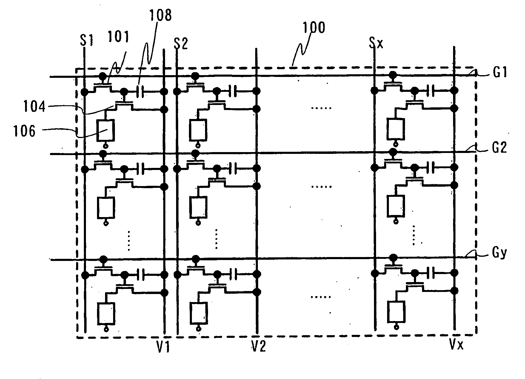
[0204]A pixel of row one and column one of the pixel portion includes the gate signal line G1, the source signal line S1, a power supply line Vx1, a power supply line Vy1, the switching TFT 1001, the driving TFT 1002, the EL element 1003, and the capacitor 1004.

[0205]Description is made on a connection between the pixel and circuit. The gate signal line G1 is connected to the gate electrode of the switching TFT 1001, the source signal line S1 is connected to the source electrode or the drain electrode of the switching TFT 1001, the power supply line Vx1 is connected to the source electrode or the drain electrode of the driving TFT 1002 and one electrode of the capacito...

embodiment mode 3

[0225]Description is made with reference to FIGS. 10, 16A and 16B on an embodiment mode of the invention.

[0226]In FIG. 10, a circuit 1054 in each pixel is described as the circuit shown in FIGS. 16A and 16B. However, this is only an example and the circuit in each pixel is not limited to the circuit in FIGS. 16A and 16B.

[0227]A pixel of row one and column one of the pixel portion includes the gate signal line G1, the source signal line S1, the power supply line Vx1, a power supply line Vy1R, the switching TFT 1001, the driving TFT 1002, the EL element 1003, and the capacitor 1004.

[0228]Description is made on a connection between the pixel and circuit. The gate signal line G1 is connected to the gate electrode of the switching TFT 1001 and the source signal line S1 is connected to the source electrode or the drain electrode of the switching TFT 1001. The power supply line Vx1 is connected to the source electrode or the drain electrode of the driving TFT 1002 and one electrode of the ...


PUM


Abstract

The invention provides an active matrix EL display device which can perform a clear multi-gray scale color display. In particular, the invention provides a large active matrix EL display device at low cost by a manufacturing method which can selectively form a pattern. Power supply lines in a pixel portion are arranged in matrix by the manufacturing method which can selectively form a pattern. Further, capacitance between wirings is reduced by providing a longer distance between adjacent wirings by the manufacturing method which can selectively form a pattern.

Description

TECHNICAL FIELD[0001]The present invention relates to an electronic display (electro-optic device) in which EL (electroluminescence) elements are formed over a substrate. In particular, the invention relates to a display device using a semiconductor element (element using a semiconductor thin film). Further, the invention relates to an electronic device using an EL display device in a display portion.BACKGROUND ART[0002]In recent years, a technique to form a thin film transistor (hereinafter referred to as a TFT in this specification) over a substrate has been drastically advanced and developed for an application to an active matrix display device. In particular, a TFT using a polycrystalline semiconductor film such as polysilicon is higher than a conventional TFT using an amorphous semiconductor film such as amorphous silicon in field effect mobility (also referred to as mobility), which enables a fast operation. Accordingly, pixels which are conventionally controlled by a driver c...

Claims


Application Information

Patent Timeline
Patent Type & Authority Applications(United States)
IPC IPC(8): G09G3/12H01J9/00
CPCH01L21/288H01L21/76838H01L27/3248H01L27/1292H01L27/156H01L27/1285H01L27/3276H10K59/123H10K59/131H01L27/1214H01L27/124
Inventor YOSHIDA, YASUNORIKIMURA, HAJIMEMAEKAWA, SHINJINAKAMURA, OSAMUYAMAZAKI, SHUNPEI
Owner SEMICON ENERGY LAB CO LTD
Why Eureka
Try Eureka