Semiconductor device

a technology of semiconductors and circuits, applied in the direction of pulse techniques, radio-controlled devices, instruments, etc., can solve the problems of deteriorating circuit performance, increasing the number of wirings and power consumption, and increasing so as to reduce the area of driving circuits, reduce the scale of circuits, and reduce the effect of circuit scal

Active Publication Date: 2008-10-16
SONY SEMICON SOLUTIONS CORP
View PDF9 Cites 9 Cited by
  • Summary
  • Abstract
  • Description
  • Claims
  • Application Information

AI Technical Summary

Benefits of technology

[0009]In an embodiment of the invention, the driving circuit can be arranged on one side of the circuit that has a delay, and the auxiliary driving circuit which accelerates the drive of the driving circuit can be arranged on the other side of the circuit that has a delay. Therefore, the area of the driving circuit is reduced as well as the auxiliary driving circuit accelerates the drive of the driving circuit, allowing the implementation of high speed drive of the circuit that has a delay.
[0010]According to an embodiment of the invention, the auxiliary driving circuit is arranged which accelerates the drive of the driving circuit and receives the drive signal of the dri...

Problems solved by technology

In drive on both ends in which a distributed constant load is driven from both ends, high speed signal transmission is realized, but a disadvantage occurs that a large scale address decoder and logic circuit cause an area increase to be noticeable.
Furtherm...

Method used


Image

  • Semiconductor device
  • Semiconductor device
  • Semiconductor device

Examples


Embodiment Construction

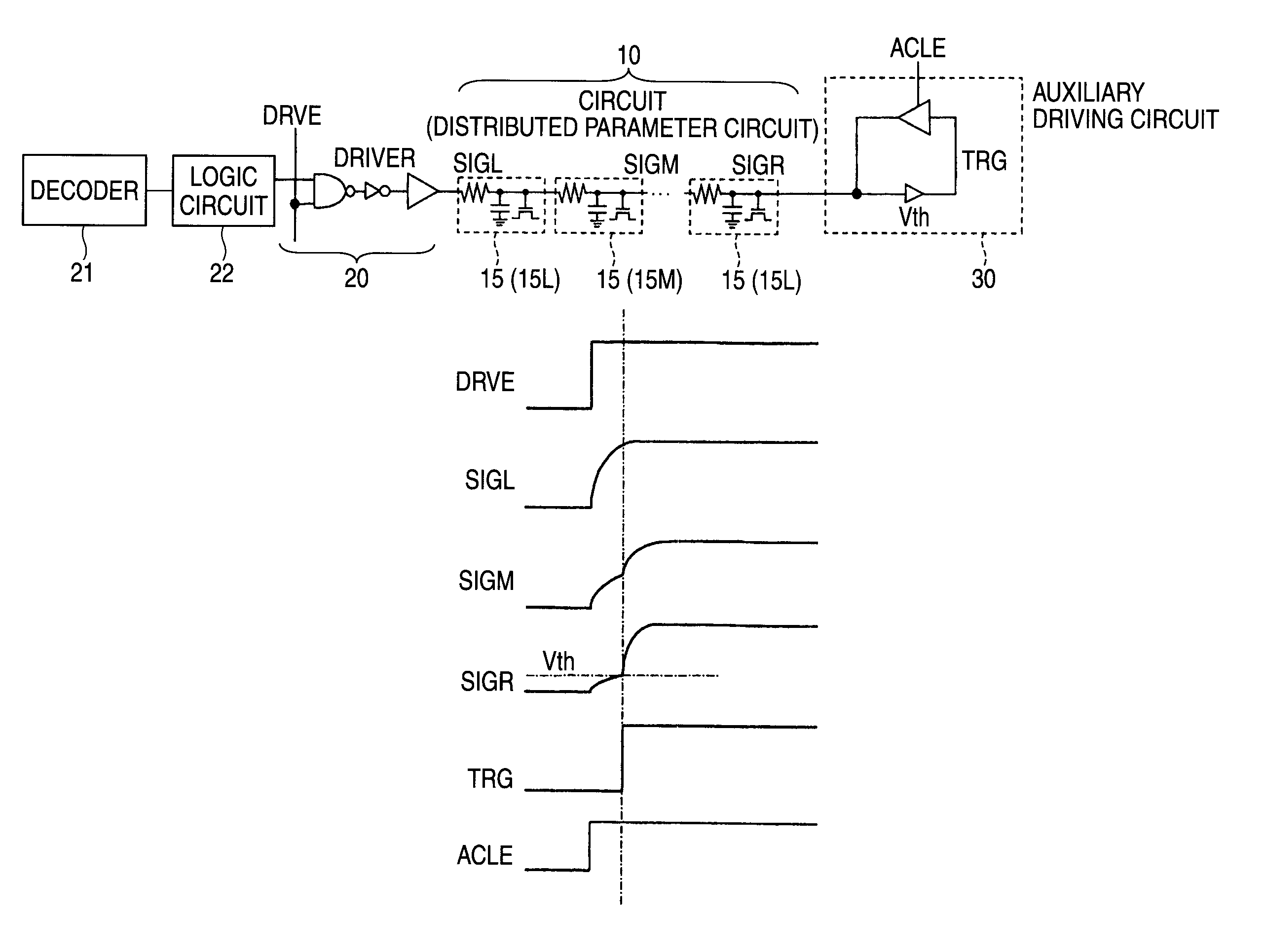
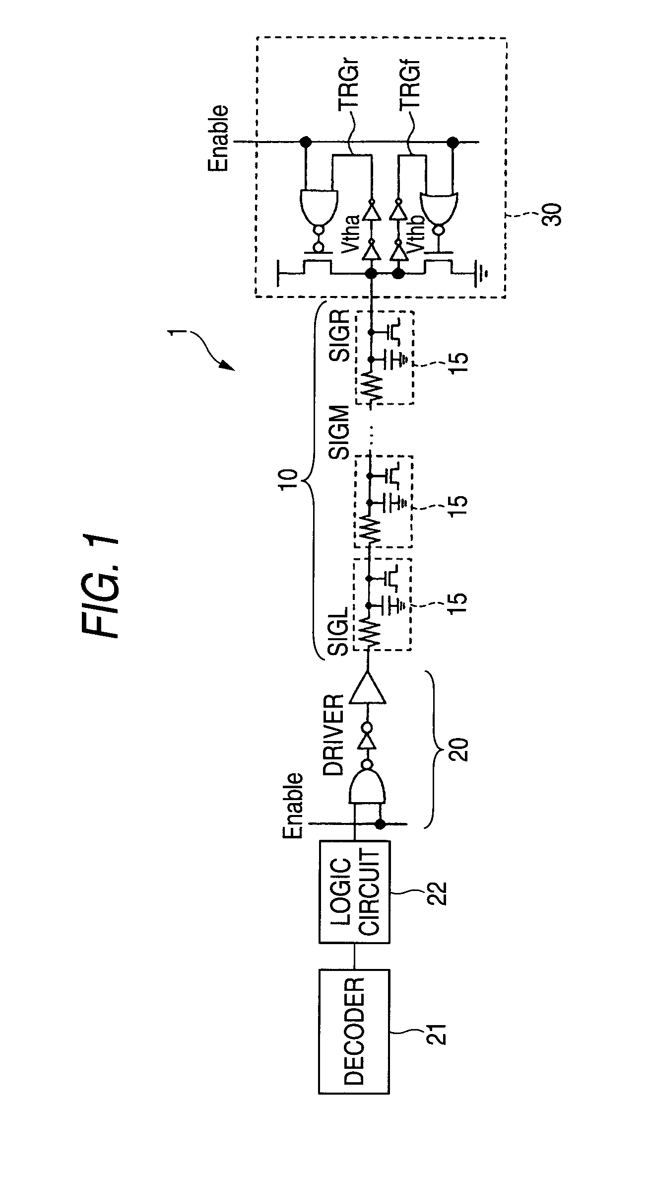
[0035]An embodiment of the invention will be described with reference to a block diagram shown in FIG. 1.

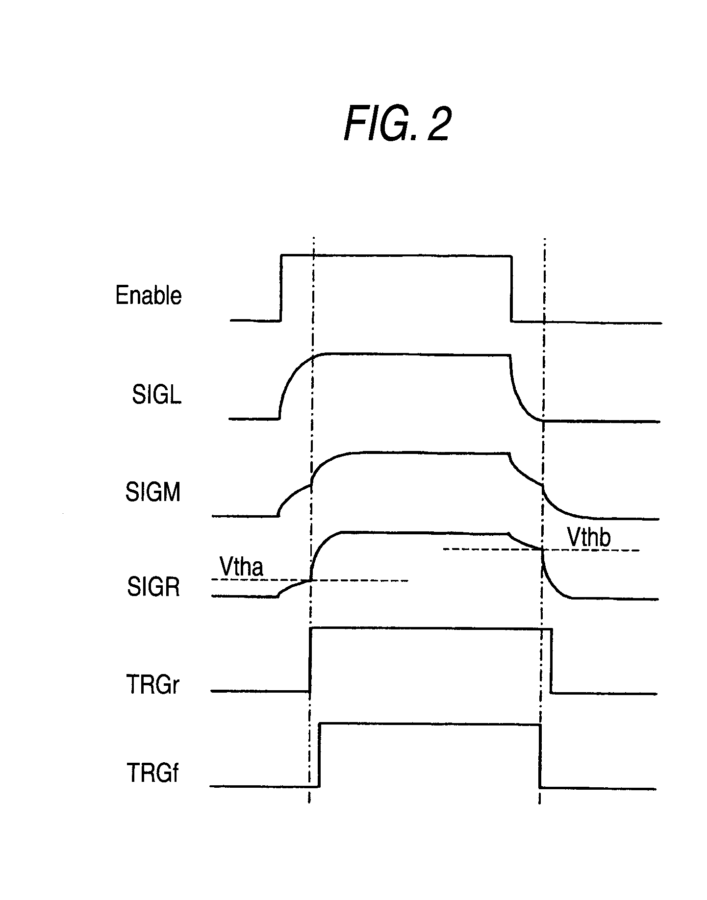
[0036]As shown in FIG. 1, a semiconductor device 1 has a circuit 10 (for example, a distributed parameter circuit). A driving circuit 20 operable to drive the circuit 10 is connected to one end of the circuit, and an auxiliary driving circuit 30 operable to accelerate the drive of the driving circuit 20 is connected to the other end of the circuit 10, which receives the drive signal of the driving circuit 20 as an input signal. As one example, the auxiliary driving circuit 30 receives the drive signal of the circuit 10 as an input signal at a level sense circuit (one of NOT elements) formed of a logic having a logic threshold Vtha, an output signal and an Enable signal of the level sense circuit enter an NAND circuit, and an output signal of the NAND circuit enters the gate of a MOS transistor to turn to the ON state to rise drive. Furthermore, it receives the drive signal of the...


PUM


Abstract

A semiconductor device is provided which has a driving circuit operable to drive a circuit that has a delay, the semiconductor device including: an auxiliary driving circuit operable to accelerate drive of the driving circuit, which receives a drive signal of the driving circuit as an input signal.

Description

CROSS REFERENCES TO RELATED APPLICATIONS[0001]The present invention contains subject matter related to Japanese Patent Application JP 2006-049730 filed in the Japanese Patent Office on Feb. 27, 2006, the entire contents of which being incorporated herein by reference.BACKGROUND OF THE INVENTION[0002]1. Field of the Invention[0003]The present invention relates to a semiconductor device having a means for accelerating drive (or the invention belongs to the field of a semiconductor device).[0004]2. Description of the Related Art[0005]Most of control signals for a solid state imaging device (CMOS image sensor, CCD), a storage device (SRAM, DRAM, ROM, a flash memory, etc.), a programmable logic array (PLA) and so on are formed from a distributed parameter circuit, and the position of driving circuits is usually limited to the end of a control signal line because of its arrangement structure. Therefore, in the drive of the distributed parameter circuit, the difference in the delay time of...

Claims


Application Information

Patent Timeline
IPC IPC(8): H03K17/04H03K5/14
CPCG11C7/12G11C8/08H03K19/01H03K3/356165H03K17/04G11C11/4085H01L27/146H04N25/71H04N25/75H04N25/76
Inventor OIKE, YUSUKE
Owner SONY SEMICON SOLUTIONS CORP
Why Eureka
Try Eureka