
SDRAM convolutional interleaver with two paths

a convolutional interleaver and ram technology, applied in the field of data communication, can solve the problems of non-volatile memory either costing more or worse, and any thing contained in ram is lost,

Active Publication Date: 2008-10-16
IMAGINE COMM
View PDF14 Cites 37 Cited by
  • Summary
  • Abstract
  • Description
  • Claims
  • Application Information

AI Technical Summary

Benefits of technology

[0121]According to a feature of the invention, a small SRAM is used to reorder and store SDRAM data such that the SDRAM access can be optimized so that a dual path Convolutional Interleaver can be implemented efficiently.
[0125]According to a feature of the invention, dual path Interleaver data is stored by writing the data in a staggered pattern such that a linear read can be done. Further this provides an advantage that write address changes are faster than read address changes during a Burst sequence.
[0129]According to another embodiment of the invention, before writing to SDRAM, data for four FEC symbols at a time may be accumulated; and then writing four symbols wide to optimize SDRAM access time. The FEC symbols may be 8 bits; and data may be written 32 bits at a time to SDRAM to fit the SDRAM interface. Two interleaver paths may be provided. Prior to packing, the symbols may be sorted to minimize a number of breaks in a sequential interleaver write address, thereby enhancing performance.

Problems solved by technology

The most widely used form of primary storage today is a volatile form of random access memory (RAM), meaning that when the computer is shut down, anything contained in RAM is lost.
Unfortunately most forms of non-volatile memory have limitations which make it unsuitable for use as primary storage.
Typically non-volatile memory either costs more or performs worse than volatile random access memory.
Memory cells alone would be worthless without some way to get information in and out of them.
SRAM is often found on microcontroller boards, either on-or off the CPU-chip because for such applications the amount of memory required is small and it would not pay off to build the extra interface circuitry for DRAMs.
The ugly thing about a storage cell is that is it leaks.
The disadvantage of the extra circuitry required for refreshing is easily offset by the lower price per bit when using large memory sizes.
A major difference between SRAM and DRAM, however, lies in the addressing technique.
With DRAM technology this simple approach is impossible since addressing a row of data without rewriting it will destruct all data in the row because of the dynamic nature.
It is clear that this is a simple but not a very efficient approach.
As real-world capacitors are not ideal and hence leak electrons, the information eventually fades unless the capacitor charge is refreshed periodically.
The most widely used form of primary storage today is a volatile form of random access memory (RAM), meaning that when the computer is shut down, anything contained in RAM is lost.
Unfortunately most forms of non-volatile memory have limitations which make it unsuitable for use as primary storage.
Typically non-volatile memory either costs more or performs worse than volatile random access memory.

Method used


Image

  • SDRAM convolutional interleaver with two paths
  • SDRAM convolutional interleaver with two paths
  • SDRAM convolutional interleaver with two paths

Examples


Embodiment Construction

[0147]According to the invention, generally, a two (2) path interleaver is set up with multiple channels, and each channel can go through a short path or a long path and perform at high speed due to the channel sorting in SRAM. Further, staggered writes to the SRAM allows the SRAM to be small, which is beneficial when implemented in FPGA. Additionally, the writes are packed to support many interleaver modes with the small SRAM. The techniques disclosed herein support having two interleaver lengths without resulting in a tremendous slowdown and dual SDRAM.

[0148]The present invention makes it possible to implement a SDRAM Convolutional Interleaver with two paths (A and B) by using SDRAM, FPGA logic and FPGA SRAM.

[0149]A problem being addressed by the present invention is that Burst writes to a SDRAM two path interleaver would max out at (be limited to) a throughput of 10 M Symbols / sec, and a higher symbol rate (such as 110 M Symbols / sec) is desired.

[0150]According to the invention, th...


PUM


Abstract

An SDRAM convolutional interleaver with two paths. Symbols are assigned to a given one of the two paths, then are sorted to minimize (to one) a number of breaks in a sequential Interleaver write address. After sorting, the symbols are stored staggered in SRAM and burst written to SDRAM. Before writing to SDRAM, data is accumulated for four symbols at a time, and the data is written four symbols wide to optimize SDRAM access time. 8 bit symbols are written 32 bits at a time to SDRAM.

Description

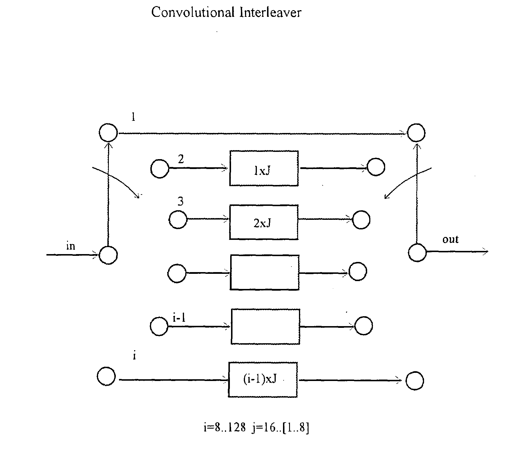
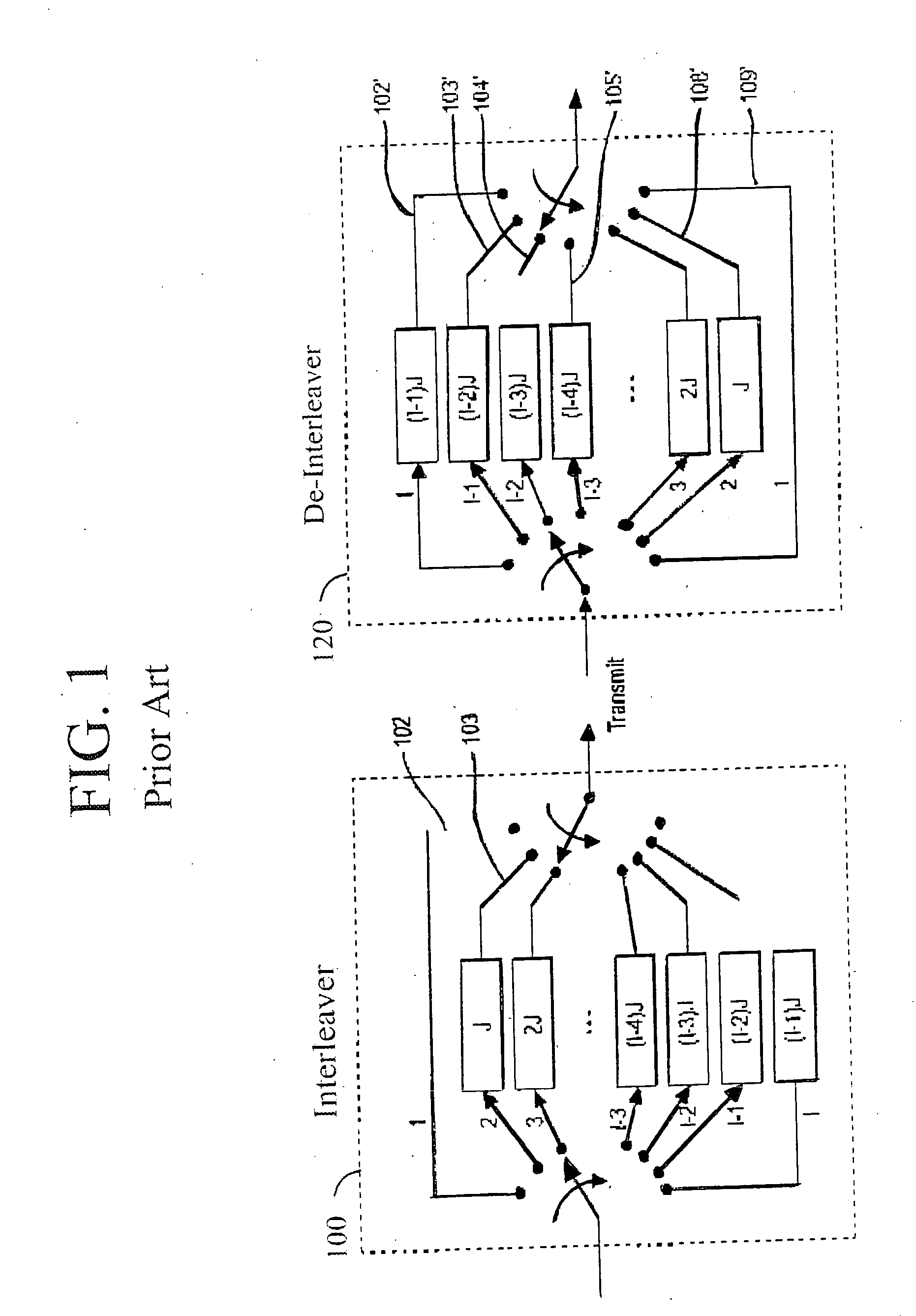
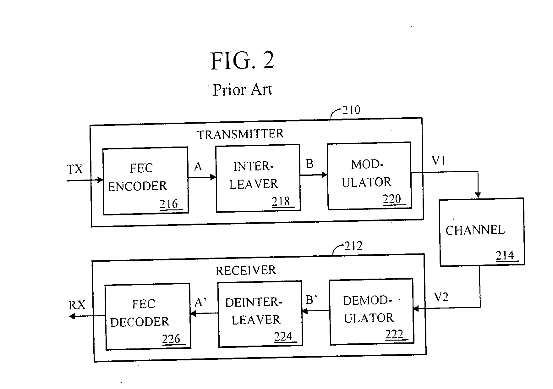
TECHNICAL FIELD OF THE INVENTION[0001]The invention relates to data communications, more particularly to error correction techniques and, more particularly to convolutional interleaving.BACKGROUND OF THE INVENTION[0002]The world is going digital. Cell phone communications are an example of digital signal communications, and satellite broadcasts are typically digital. Many wired telephone connections are still analog, as are most television broadcasts, but it not inconceivable that these medium will also move towards digital, and analog signals for communication will largely be a thing of the past.[0003]In parallel with the “digital revolution”, the world is going wireless. Cell phones are an example of wireless communication.[0004]The whole field of digital communications has spawned several areas of specialty and expertise, including error detection and correction techniques, to name a few.[0005]“Coding” is a term that often shows up in any discussion of digital signal processing. ...

Claims


Application Information

Patent Timeline
Patent Type & Authority Applications(United States)
IPC IPC(8): H03M13/07
CPCH03M13/15H03M13/1515H03M13/2732
Inventor ANDERSSON, JORGEN
Owner IMAGINE COMM
Learn More