Semiconductor chip and semiconductor device

a semiconductor chip and chip technology, applied in semiconductor devices, semiconductor/solid-state device details, electrical equipment, etc., can solve the problems of increasing increasing the power noise of lsi, and reducing the power voltage. , to achieve the effect of reducing the number of c4 solder balls and reducing the number of signal bumps or power bumps connectables

Inactive Publication Date: 2008-10-23
HITACHI LTD
View PDF4 Cites 60 Cited by
  • Summary
  • Abstract
  • Description
  • Claims
  • Application Information

AI Technical Summary

Benefits of technology

[0039](1) The capacitor is mounted on a back surface of the chip, thereby solving the problem of largely reducing the number of signal bumps or power bumps connectable to a pa

Problems solved by technology

According to developments, improvement in speed and improvement in functionality of semiconductor device (LSI) processes, the power noise of LSI has been increased.
This is because a power voltage is decreased as the semiconduct

Method used


Image

  • Semiconductor chip and semiconductor device
  • Semiconductor chip and semiconductor device
  • Semiconductor chip and semiconductor device

Examples


first embodiment

[0067]A first embodiment of the present invention will be described with reference to FIG. 1 to FIG. 6.

[0068]Described in the present embodiment is about power noise that influences a semiconductor chip in a semiconductor device. Although signals and signal wirings are not described in the drawings for the sake of easy view, they are included in the actual products, and they will be described as needed herein after.

[0069]And, in the following description, the semiconductor chip may be described as a chip, the decoupling capacitor may be capacitor or a chip capacitor, and a semiconductor package may be described as a package, a semiconductor interposer, or an interposer. Moreover, an electrode may be described as a pad, a C4 solder ball may be described as a solder ball or a bump.

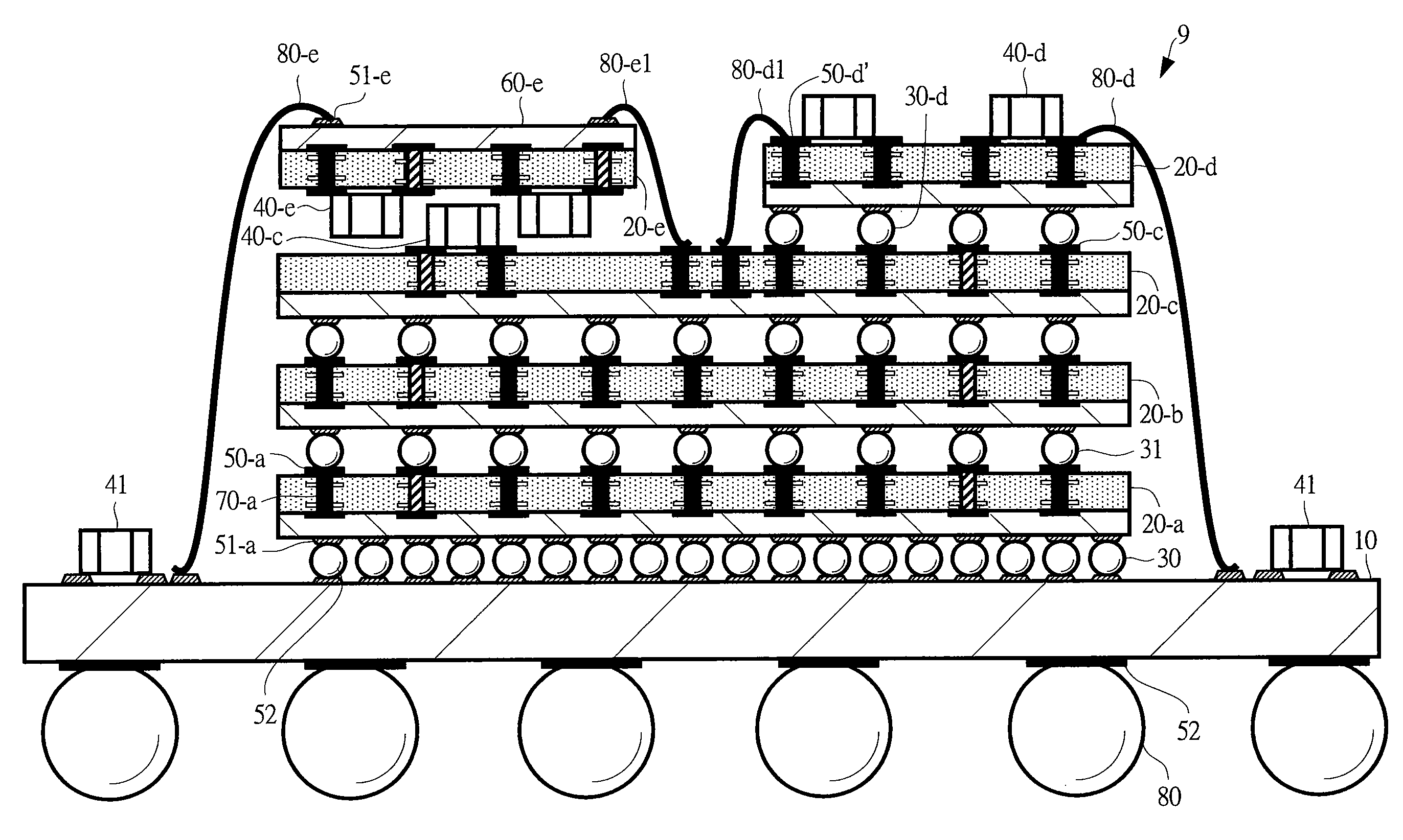
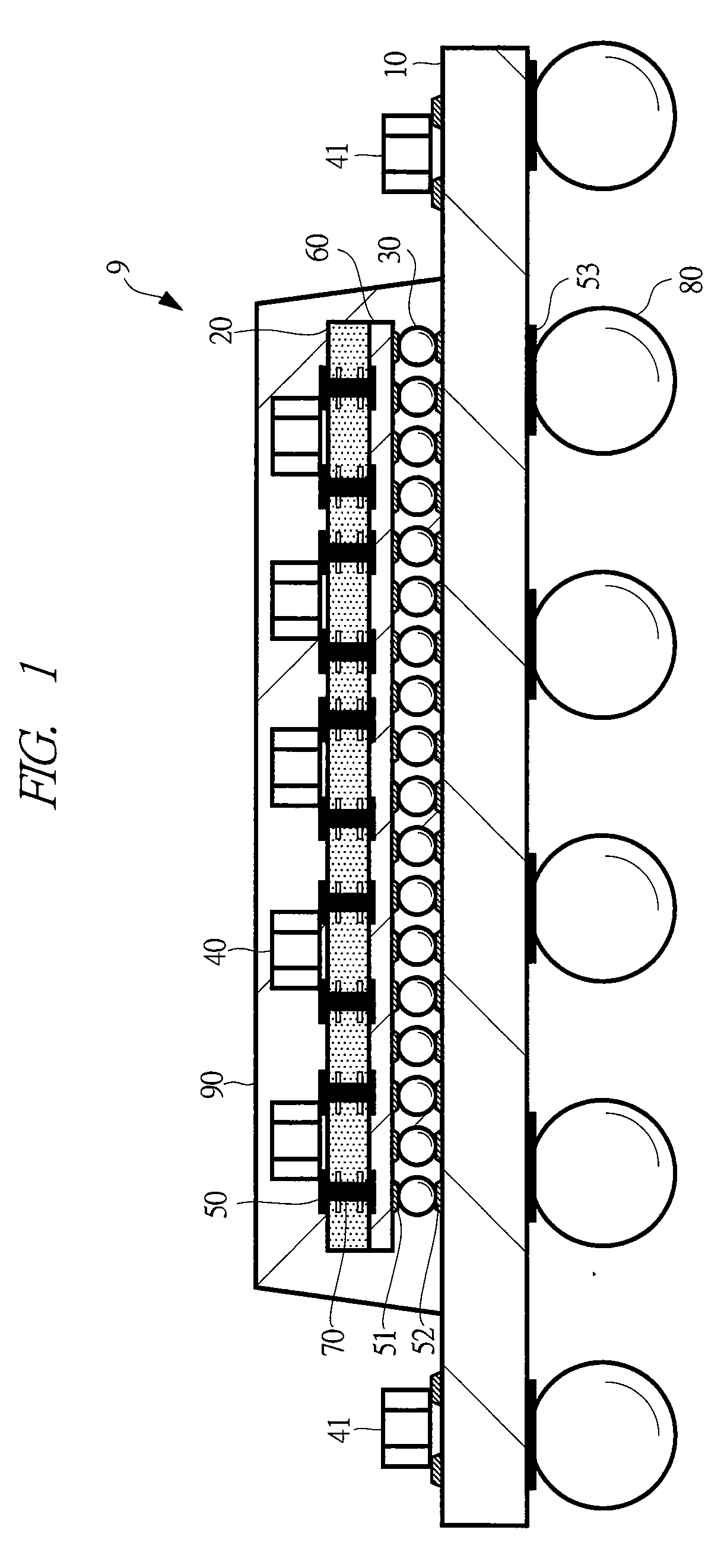
[0070]FIG. 1 shows a cross-sectional view of the semiconductor device according to the present embodiment. A circuit function for information processing is mounted to a semiconductor device (LSI) 9. The semi...

second embodiment

[0093]A second embodiment of the present invention will be described with reference to FIG. 7.

[0094]The present embodiment is, similarly to the first embodiment, an example where the capacitor 40 is mounted on the back surface of the semiconductor chip 20. A difference from the first embodiment lies in that the applied voltage to the capacitor 40 is sectioned by the kinds of power supplies.

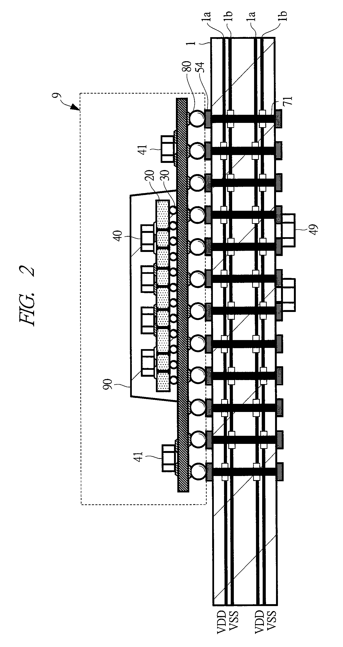
[0095]FIG. 7A is a top view showing the wiring layer side (surface) of the semiconductor chip 20, and blocks (areas) of the circuits formed on the semiconductor chip 20 are denoted by 21 to 25. While there are five functional blocks to which different powers are supplied are described in FIG. 7A, the number may be larger or smaller.

[0096]Electrodes 51-1 to 51-5 for the C4 solder ball 30 are arranged in a reticular pattern on the upper surface of the semiconductor chip 20. The areas 21 to 25 are blocks having input / output interface circuit functions of different signals, and a signal and power are ...

third embodiment

[0102]A third embodiment of the present invention will be described with reference to FIGS. 8A and 8B.

[0103]The present embodiment is, similarly to the second embodiment, an example where the capacitor is mounted on the back surface of the semiconductor chip 20 per area. In addition, this is an example where a resistor (R) 40-6 having an almost same size as the capacitor is additionally mounted on the back surface of the semiconductor chip 20 to configure a filter.

[0104]An area 26 in FIG. 8A is an analog circuit unit such as a PLL configured by the wiring layer 60 of the semiconductor chip 20. The power of the area 26 is connected to the power wiring in the wiring layer 60 by a via hole, and connected to an electrode 50-6 of the back surface of the semiconductor chip 20 by the via hole. And, the resistor (R) 40-6 and a capacitor (C) 40-7 are connected to the electrode 50-6, thereby configuring a low-pass filter (LPF). Although not shown, a capacitor is mounted also to the area 25. I...


PUM


Abstract

A semiconductor chip and a semiconductor device mounting the semiconductor chip capable of increasing a capacitance of a capacitor without reducing the number of signal bumps or power bumps of a package and the number of C4 solder balls of the semiconductor chip, and achieving a stable power supply with suppressing fluctuations of power at a resonance frequency without a limitation in a position to mount a capacitor for lowering noise of a signal transceiving interface block. In the semiconductor device, a via hole is provided to the semiconductor chip, a power-supply electrode connected to the via hole is provided to a back surface of the semiconductor chip, and a capacitor is mounted to the electrode on the back surface. And, a high-resistance material is used for a material of a power-supply via hole inside the semiconductor chip, thereby increasing the resistance and lowering the Q factor.

Description

CROSS-REFERENCE TO RELATED APPLICATION[0001]The present application claims priority from Japanese Patent Application No. JP 2007-112574 filed on Apr. 23, 2007, the content of which is hereby incorporated by reference into this application.TECHNICAL FIELD OF THE INVENTION[0002]The present invention relates to a technique for a semiconductor chip and a semiconductor device mounting the same. More particularly, the present invention relates to a technique effectively applied to a semiconductor device mounting a functional circuit and application products of the semiconductor device including information processing devices such as a personal computer, server, router and storage, and a processor and a memory embedded in information home appliances such as an information in-vehicle terminal, television and camera.BACKGROUND OF THE INVENTION[0003]According to developments, improvement in speed and improvement in functionality of semiconductor device (LSI) processes, the power noise of LSI ...

Claims


Application Information

Patent Timeline
IPC IPC(8): H01L45/00
CPCH01L23/481H01L23/50H01L23/642H01L24/49H01L24/73H01L25/0657H01L2224/48091H01L2224/48227H01L2224/49171H01L2225/06513H01L2225/06517H01L2225/06541H01L2225/06572H01L2924/01004H01L2924/01005H01L2924/01013H01L2924/01029H01L2924/01073H01L2924/01074H01L2924/01077H01L2924/15311H01L2924/19041H01L2924/19042H01L2924/19043H01L2924/19105H01L2924/19107H01L2924/30105H01L2924/30107H01L2924/3011H01L2924/3025H01L2924/00014H01L24/48H01L2924/01006H01L2924/01023H01L2924/01033H01L2924/014H01L2224/16145H01L2224/16225H01L2924/00Y10S257/904Y10S257/924H01L2224/73257H01L2924/12041H01L2924/181H01L2224/05573H01L2224/05568H01L2224/48145H01L2924/19104H01L2224/0554H01L25/16H01L2224/17181H01L2224/45099H01L2224/05599H01L2924/00012H01L2224/0555H01L2224/0556
Inventor OSAKA, HIDEKISAITO, TATSUYA
Owner HITACHI LTD
Why Eureka
Try Eureka