

Method of making semiconductor device
a technology of semiconductor devices and plasma, which is applied in the direction of electrical equipment, basic electric elements, electric discharge tubes, etc., can solve the problems of reducing the etching rate of the physical etching of the hard mask by the plasma of noble gas, and achieve the effect of improving the controllability of the etching of the high-dielectric-constant insulating film
- Summary
- Abstract
- Description
- Claims
- Application Information
AI Technical Summary
Benefits of technology
Problems solved by technology
Method used
Image

Examples
example 1
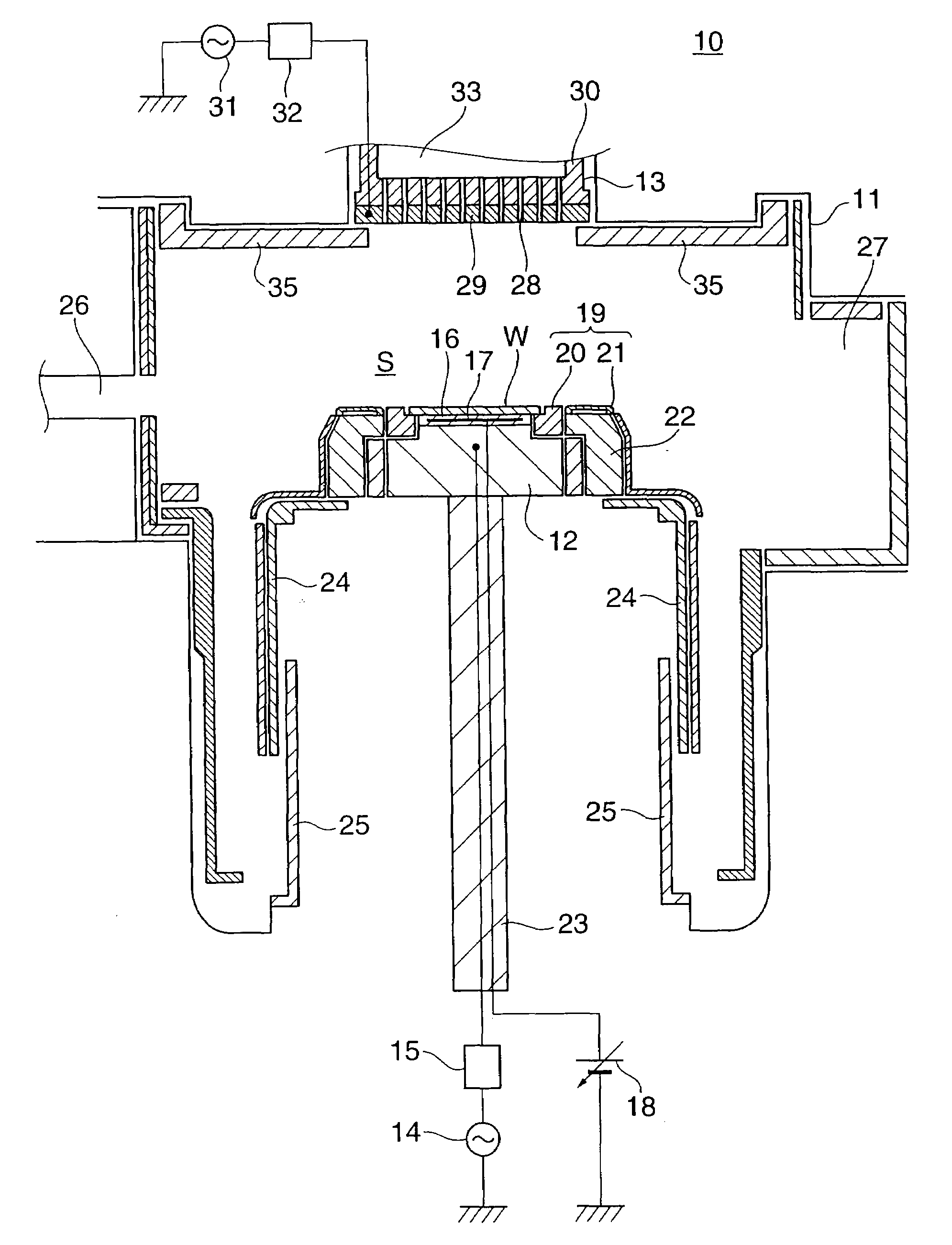
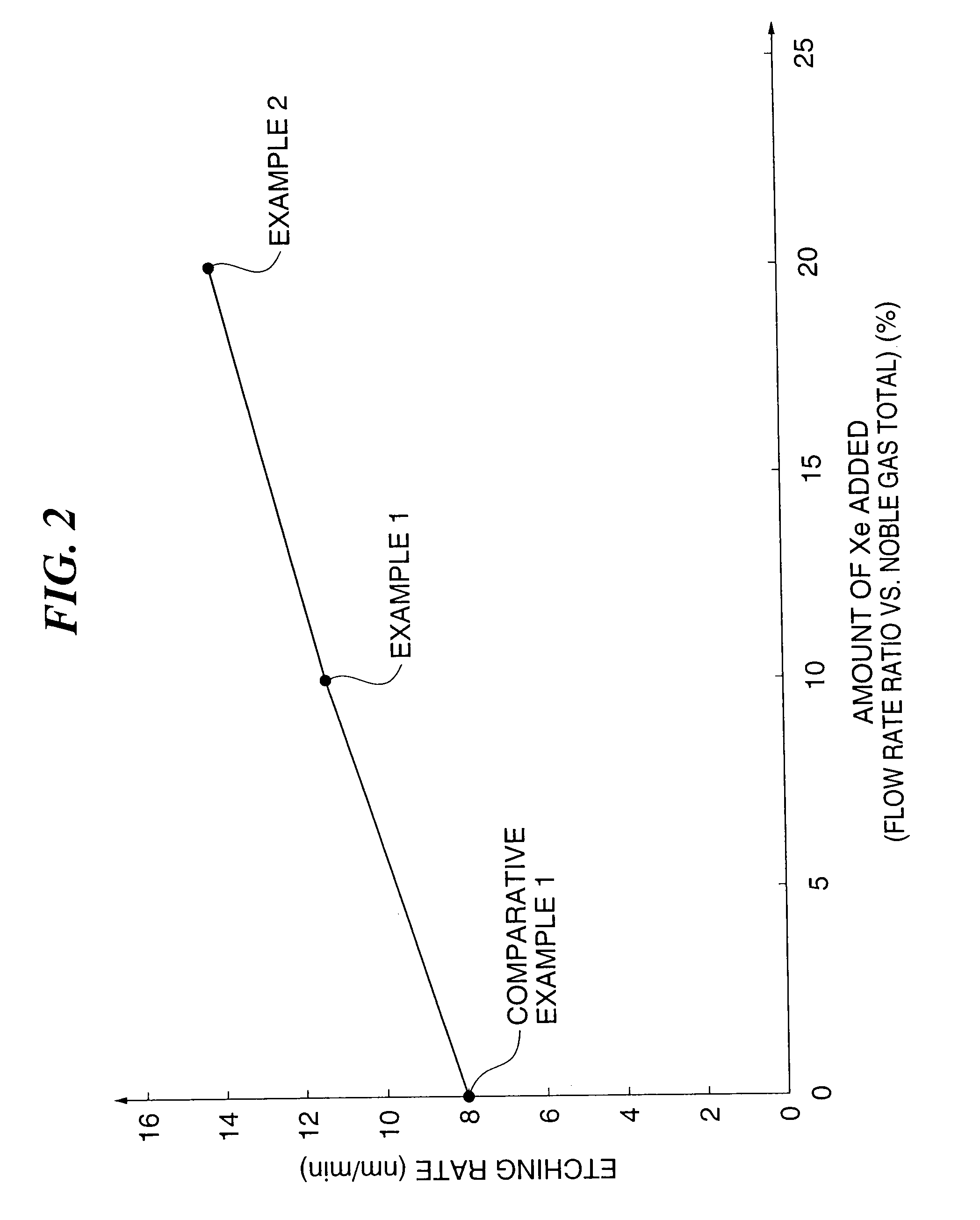
[0079]First, a hafnium oxide film blanket wafer (a wafer having a hafnium oxide film formed on a surface thereof in the form of a blanket) was prepared as a wafer to be etched. Next, the blanket wafer was transferred into the chamber 11 of the plasma processing apparatus 10, and a mixture of C4F8 gas, carbon monoxide gas, argon gas and xenon gas at flow rates of 27, 300, 540 and 60 sccm respectively was supplied into the processing space S in the chamber 11 as a processing gas. The amount added of xenon relative to the total amount of noble gas was thus 10% in terms of the flow rate ratio. Next, high-frequency electrical power was applied into the processing space S, thus producing a plasma from the processing gas supplied, and hence etching the blanket wafer. The etching rate was measured during the etching. The measured etching rate is shown on a graph in FIG. 2.
example 2
[0080]First, a hafnium oxide film blanket wafer was prepared as in Example 1. Next, the blanket wafer was etched using the same method as in Example 1. Here, a mixture of C4F8 gas, carbon monoxide gas, argon gas and xenon gas at flow rates of 27, 300, 480 and 120 sccm respectively was supplied into the processing space S. The amount added of xenon relative to the total amount of noble gas was thus 20% in terms of the flow rate ratio. The measured etching rate is shown on the graph in FIG. 2.
[0081]Moreover, a wafer having a hafnium oxide film formed on an Si layer either directly or with an SiO2 layer therebetween was etched under the same etching conditions as stated above for this example, and the surface form of the etched wafer was measured. A sectional view of the measured form is shown in FIG. 3B.
example 3
[0085]First, a hafnium oxide film blanket wafer, a silicon nitride film blanket wafer, and an SiO2 film blanket wafer were prepared as wafers to be etched. Next, each of the wafers in turn was transferred into the chamber 11 of the plasma processing apparatus 10, and a mixture of argon gas, xenon gas and hydrogen gas at flow rates of 180, 420 and 4 sccm respectively was supplied into the processing space S in the chamber 11 as a processing gas. Next, high-frequency electrical power was applied into the processing space S, thus producing a plasma from the processing gas, and hence etching the wafer. The etching rate was measured during the etching. The measured etching rates are shown on a graph in FIG. 4. Moreover, the etching selectivity ratio for the hafnium oxide film versus the silicon nitride film, and the etching selectivity ratio for the hafnium oxide film versus the SiO2 film are shown on a graph in FIG. 5.
PUM
| Property | Measurement | Unit |
|---|---|---|
| diameter | aaaaa | aaaaa |
| current | aaaaa | aaaaa |
| etching rate | aaaaa | aaaaa |
Abstract
Description
Claims
Application Information